BA17805T Ver la hoja de datos (PDF) - ROHM Semiconductor
Número de pieza
componentes Descripción
Fabricante
BA17805T Datasheet PDF : 11 Pages
| |||
Regulator ICs
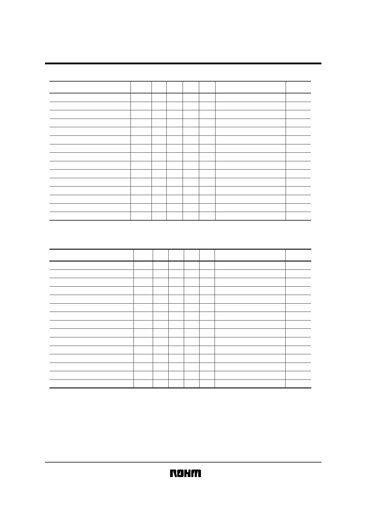
BA178!!T / FP series
<BA17810T / FP individual specifications> (unless otherwise noted, Ta=25°C, VIN=16V, IO=500mA)
Parameter
Output voltage 1
Symbol Min. Typ. Max. Unit
Conditions
VO1 9.6 10.0 10.4 V IO=500mA
Measurement
circuit
Fig.1
Output voltage 2
VO2
9.5
− 10.5 V VIN=12.5∼25V, IO=5mA∼1A
Fig.1
Input stability 1
Reg.I1 −
7 200 mV VIN=12.5∼27V, IO=500mA
Fig.1
Input stability 2
Reg.I2 −
4 100 mV VIN=14∼20V, IO=500mA
Fig.1
Ripple rejection ratio
R.R. 55 64
−
dB eIN=1Vrms, f=120Hz, IO =100mA Fig.2
Load regulation 1
Reg.L1 −
21 200 mV IO=5mA∼1A
Fig.1
Load regulation 2
Reg.L2 −
Temperature coefficient of output voltage TCVO −
Output noise voltage
Vn
−
8
90 mV IO=250∼750mA
−0.5 − mV/˚C IO=5mA, Tj =0∼125˚C
100 −
µV f=10Hz∼100kHz
Fig.1
Fig.1
Fig.3
Minimum I/O voltage differential
Vd
− 2.0 −
V IO=1A
Fig.4
Bias current
Ib
−
4.5 8.0 mA IO=0mA
Fig.5
Bias current change 1
Ib1
−
−
0.5 mA IO=5mA∼1A
Fig.5
Bias current change 2
Ib2
−
−
0.8 mA VIN=12.5∼27V
Fig.5
Peak output current
Output short-circuit current
IO-P
−
1.7
−
IOS
− 0.3 −
A Tj=25˚C
A VIN=30V
Fig.1
Fig.6
<BA17812T / FP individual specifications> (unless otherwise noted, Ta=25°C, VIN=19V, IO=500mA)
Parameter
Symbol
Output voltage 1
VO1
Output voltage 2
VO2
Input stability 1
Reg.I1
Input stability 2
Reg.I2
Ripple rejection ratio
R.R.
Load regulation 1
Reg.L1
Load regulation 2
Reg.L2
Temperature coefficient of output voltage TCVO
Output noise voltage
Vn
Minimum I/O voltage differential
Vd
Bias current
Ib
Bias current change 1
Ib1
Bias current change 2
Ib2
Peak output current
IO-P
Output short-circuit current
IOS
Min.
11.5
11.4
−
−
55
−
−
−
−
−
−
−
−
−
−
Typ.
12.0
−
8
5
63
23
10
−0.5
110
2.0
4.5
−
−
1.7
0.3
Max. Unit
Conditions
12.5 V IO=500mA
12.6 V VIN=15∼27V, IO=5mA∼1A
240 mV VIN=14.5∼30V, IO=500mA
120 mV VIN=16∼22V, IO=500mA
− dB eIN=1Vrms, f=120Hz, IO =100mA
240 mV IO=5mA∼1A
120 mV IO=250∼750mA
− mV/˚C IO=5mA, Tj =0∼125˚C
− µV f=10Hz∼100kHz
−
V IO=1A
8.0 mA IO=0mA
0.5 mA IO=5mA∼1A
0.8 mA VIN=14.5∼30V
−
A Tj=25˚C
−
A VIN=30V
Measurement
circuit
Fig.1
Fig.1
Fig.1
Fig.1
Fig.2
Fig.1
Fig.1
Fig.1
Fig.3
Fig.4
Fig.5
Fig.5
Fig.5
Fig.1
Fig.6
Share Link: 