LC587006 Ver la hoja de datos (PDF) - SANYO -> Panasonic
Número de pieza
componentes Descripción
Fabricante
LC587006
SANYO -> Panasonic

LC587006 Datasheet PDF : 29 Pages
| |||
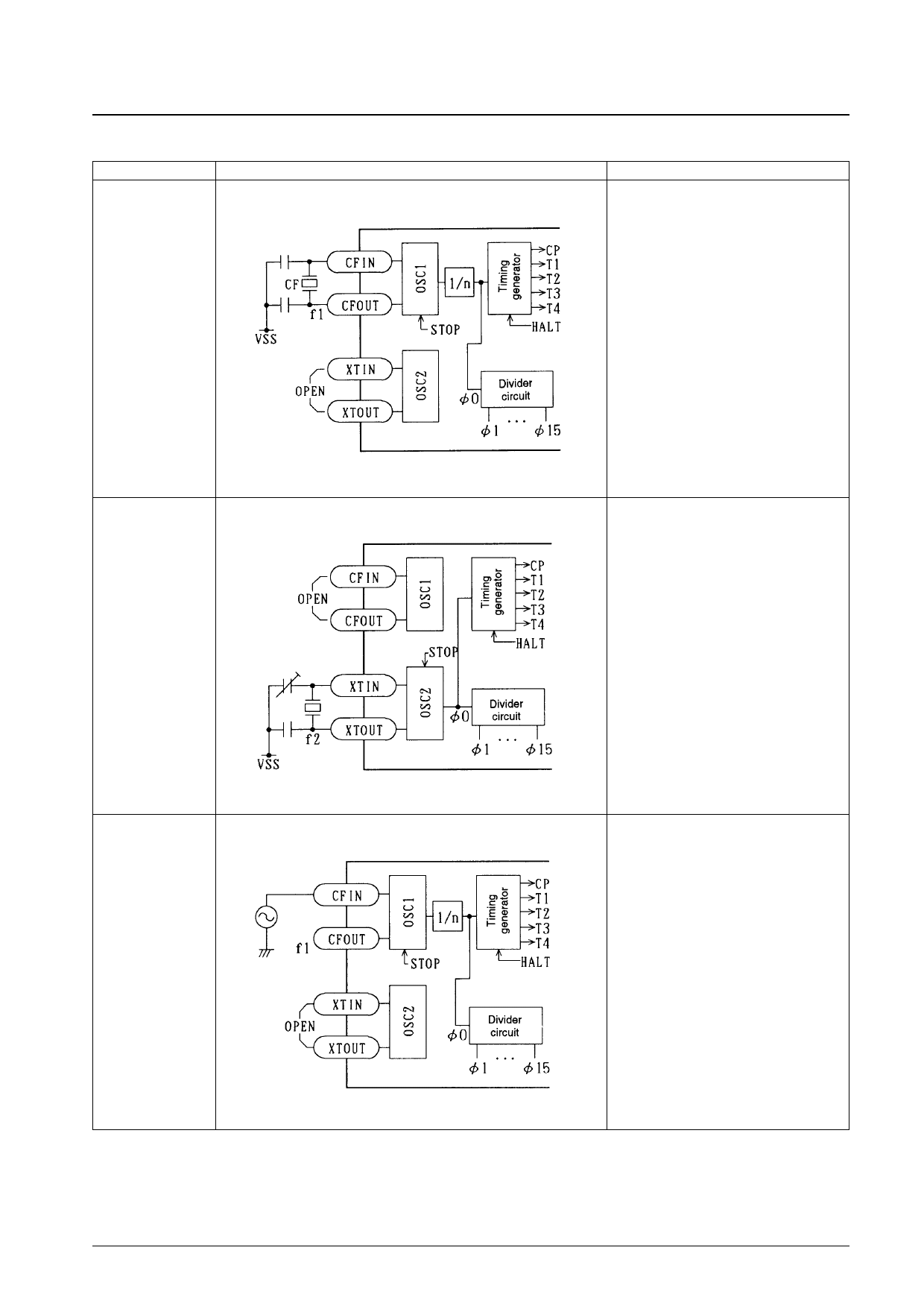
LC587008, 587006, 587004
Continued from preceding page.
Option
Circuit configuration
Note
CF
• 400 kHz
• 4 MHz
• The cycle time is four times n times the f1
period. (Note: n is 2.)
• The divider outputs (ø1 to ø15) are used as
the LCD drive waveform generation clock,
the S and K port chattering rejection clock
and for other functions.
• The cycle time is four times the f2 period.
• The divider outputs (ø1 to ø15) are used as
Xtal
the time base, the LCD drive waveform
generation clock, the S and K port
chattering rejection clock and for other
functions.
External input
• The cycle time is four times n times the f1
period. (Note: n is 2.)
• The divider outputs (ø1 to ø15) are used as
the LCD drive waveform generation clock,
the S and K port chattering rejection clock
and for other functions.
No. 4435-9/29
Share Link: