LC587004 Ver la hoja de datos (PDF) - SANYO -> Panasonic
Número de pieza
componentes Descripción
Fabricante
LC587004
SANYO -> Panasonic

LC587004 Datasheet PDF : 29 Pages
| |||
LC587008, 587006, 587004
Pin Functions
Pin
VDD
VSS
QIP-80
I/O
Pin No.
—
24
—
23
Power supply
LCD drive power supply
Function
VDD1
VDD2
—
22
—
21
Option
At reset
CUP1
CUP2
CFIN
CFOUT
XTIN
XTOUT
S1
S2
S3
S4
K1
K2
K3
K4
M1
M2
M3
M4
A1
A2
A3
A4
P1
P2
P3
P4
—
—
Input
Output
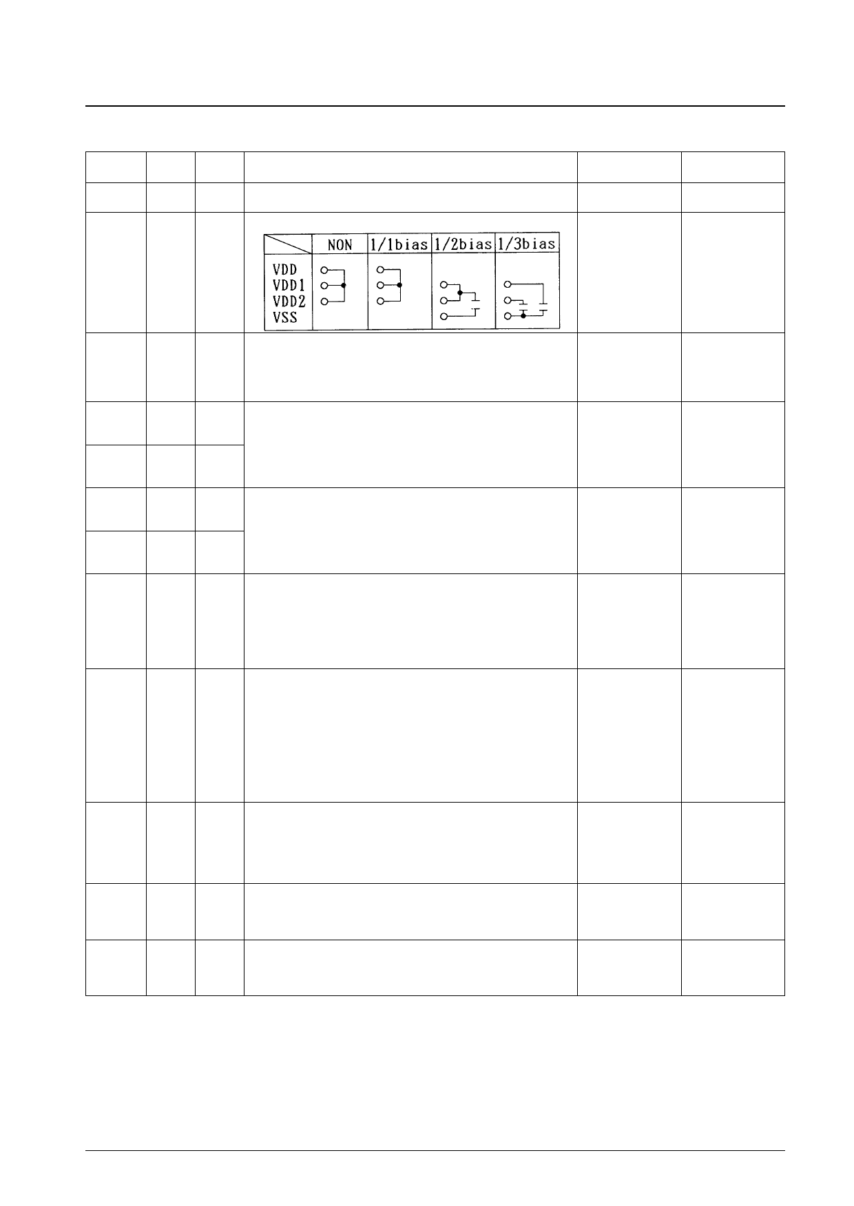
Switching pin used to supply the LCD drive voltage to the VDD1 and
3
VDD2 pins
• Connect a nonpolarized capacitor between CUP1 and CUP2 when
4
1/2 or 1/3 bias is used.
• Leave open when a bias other than 1/2 or 1/3 is used.
System clock oscillator connections
25
• Ceramic resonator connection (CF specifications)
• RC component connection (RC specifications)
• External signal input pin (CFOUT is left open)
26
This oscillator is stopped by the execution of a STOP or SLOW
instruction.
• CF specifications
• RC specifications
• External
specifications
• Not used
Input
Output
20
19
Reference calculation (clock specifications, LCD alternating frequency),
system clock oscillator
• 32 kHz crystal resonator connection
• 65 kHz crystal resonator connection
This oscillator is stopped by the execution of a STOP instruction.
• 32k specifications
• 65k specifications
• 38k specifications
• Not used
Input
I/O
I/O
I/O
I/O
Input-only ports
27
• Input pins used to read data into RAM
28
• Built-in 7.8 ms and 1.95 ms chatter rejection circuits
29
• Built-in pull-up/pull-down resistors
30
Note: The 7.8 ms and 1.95 ms times are the times when ø0 is
32.768 kHz.
• Transistors to hold
a low or high level
• Selection of either
pull-up or pull-
down resistors
• The pull-up or pull-
down resistors are
on.
Note: These pins go
to the floating
state when
reset is cleared.
I/O ports
31
• Input pins used to read data into RAM
32
• Output pins used to output data from RAM
33
• Built-in 7.8 ms and 1.95 ms input-mode chatter rejection circuits.
34
The selection of 7.8 or 1.95 ms is linked to that for the S ports.
Note: The 7.8 ms and 1.95 ms times are the times when ø0 is
32.768 kHz.
• Transistors to hold
a low or high level
• Selection of either
pull-up or pull-
down resistors
• The pull-up or pull-
down resistors are
on.
Note: These pins go
to the floating
state when
reset is cleared.
• Input mode
• Output latch data is
set high.
I/O ports
35
• Input pins used to read data into RAM
36
• Output pins used to output data from RAM
The same as K1 to The same as K1 to
37
• M4 is used as the external clock input pin in TM2 mode 3.
K4
K4
38
* The minimum period for the external clock is twice the cycle time.
• Built-in pull-up/pull-down resistors
11
I/O ports
12
• Input pins used to read data into RAM
13
• Output pins used to output data from RAM
14
• Built-in pull-up/pull-down resistors
The same as K1 to
K4
The same as K1 to
K4
15
16
I/O ports
17
Function: The same as pins A1 to A4
18
The same as K1 to
K4
The same as K1 to
K4
Continued on next page.
No. 4435-5/29
Share Link: