SG3524 Ver la hoja de datos (PDF) - STMicroelectronics
Número de pieza
componentes Descripción
Fabricante
SG3524 Datasheet PDF : 9 Pages
| |||
PRINCIPLES OF OPERATION
The SG2524/3524 is a fixed frequency pulse-
with-modulation voltage regulator control circuit.
The regulator operates at a frequency that is pro-
grammed by one timing resistor (RT) and one tim-
ing capacitor (CT). RT established a constant
charging current for CT. This results in a linear
voltage ramp at CT, which is fed to the compara-
tor providing linear control of the output pulse
width by the error amplifier. the SG2524/3524
contains, an on-board 5V regulator that serves as
a reference as well as powering the
SG2524/3524’s internal control circuitry and is
also useful in supplying external support functions.
This reference voltage is lowered externally by a
resistor divider to provide a reference within the
common mode range the error amplifier or an ex-
ternal reference may be used. The power supply
output is sensed by a second resistor divider net-
work to generale a feedback signal to error ampli-
fier. The amplifier output voltage is then com-
pared to the linear voltage ramp at CT. The
resulting modulated pulse out of the high-gain
comparator is then steered to the appropriate out-
put pass transistors (QA or QB) by the pulse-
steering flip-flop, which is synchronously toggled
by the oscillator output. The oscillator output
pulse also serves as a blanking pulse to assure
both output are never on simultaneously during
the transition times. The width of the blanking
pulse is controlled by the value of CT. The outputs
may be applied in a push-pull configuration in
which their frequency is half that of the base oscil-
lator, or paralleled for single-ended applications in
which the frequency is equal to that of the oscilla-
tor. The output of the error amplifier shares a
common input to the comparator with the current
limiting at shutdown circuitry and can be overrid-
den by signals from either of these inputs. This
common point is also available externally and
may be employed to control the gain of, or to
compensate, the error amplifier, or to provide ad-
ditional control to the regulator.
RECOMMENDED OPERATING CONDITIONS
Supply voltage VIN
Reference Output Current
Current trough CT Terminal
Timing Resistor, RT
Timing Capacitor, CT
8 to 40V
0 to 20mA
- 0.03 to -2mA
1.8 to 100KΩ
0.001 to 0.1µF
TYPICAL APPLICATIONS DATA
OSCILLATOR
The oscillator controls the frequency of the
SG2524 - SG3524
SG2524 and is programmed by RT and CT ac-
cording to the approximate formula:
f
=
1.18
RT CT
where:
RT is in KΩ
CT is in µF
f is in KHz
Pratical values of CT fall between 0.001 and
0.1µF. Pratical values of RT fall between 1.8 and
100KΩ. This results in a frequency range typically
from 120Hz to to 500KHz.
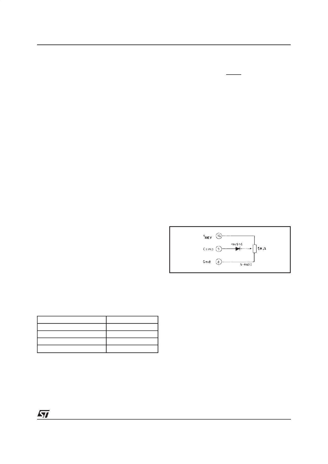
BLANKING
The output pulse of oscillator is used as a blank-
ing pulse at the output. This pulse width is con-
trolled by the value of CT.If small values of CT are
required for frequency control, the oscillator out-
put pulse width may still be increased by applying
a shunt capacitance of up to 100pF from pin 3 to
ground. If still greater dead-time is required, it
should be accomplished by limiting the maximum
duty cycle by clamping the output of the error am-
plifier. This can easily be done with the circuit be-
low:
Figure 6.
SYNCRONOUS OPERATION
When an external clock is desired, a clock pulse
of approximately 3V can be applied directly to the
oscillator output terminal. The impedance to
ground at this point is approximately 2KΩ. In this
configuration RT CT must be selected for a clock
period slightly greater than that the external clock.
If two more SG2524 regulators are to be operated
synchronously, all oscillator output terminals
should be tied together, all CT terminals con-
nected to a single timing capacitor, and timing re-
sistor connected to a single RT terminal. The
other RT terminals can be left open or shorted to
VREF. Minimum lead lengths should be used be-
tween the CT terminals.
5/9
Share Link: 