ADM1024(2000) Ver la hoja de datos (PDF) - Analog Devices
Número de pieza
componentes Descripción
Fabricante
ADM1024 Datasheet PDF : 28 Pages
| |||
ADM1024
Parameter
Min Typ Max Unit Test Conditions/Comments
SERIAL BUS DIGITAL INPUTS
(SCL, SDA)
Input High Voltage, VIH
Input Low Voltage, VIL
Hysteresis
Glitch Immunity
2.2
V
0.8 V
500
mV
100
ns
DIGITAL INPUT LOGIC LEVELS
(ADD, CI, RESET, VID0–VID4, FAN1, FAN2)
Input High Voltage, VIH
2.2
Input Low Voltage, VIL
V
0.8 V
(See Note 7)
VCC = 2.85 V – 5.5 V
VCC = 2.85 V – 5.5 V
NTEST_IN
Input High Voltage, VIH
2.2
V
VCC = 2.85 V – 5.5 V
DIGITAL INPUT CURRENT
Input High Current, IIH
Input Low Current, IIL
Input Capacitance, CIN
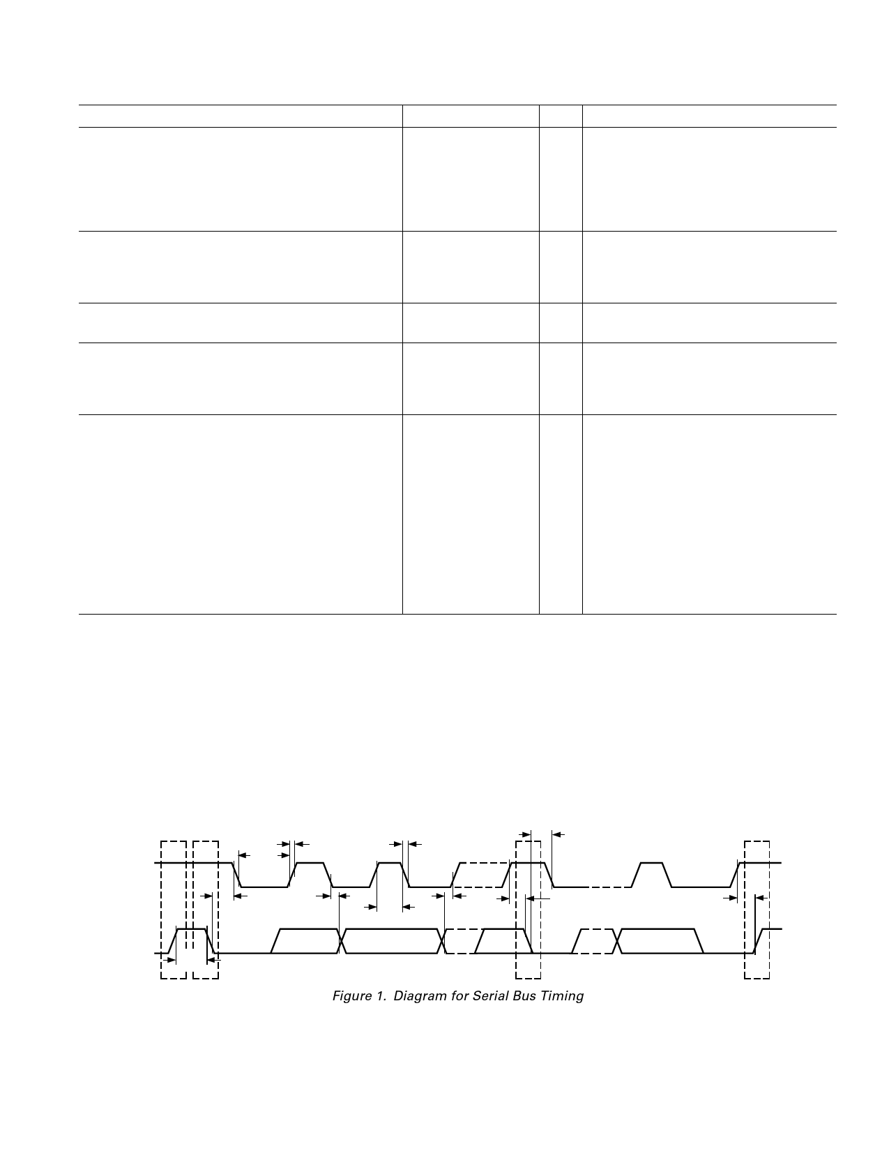
SERIAL BUS TIMING8
Clock Frequency, fSCLK
Glitch Immunity, tSW
Bus Free Time, tBUF
Start Setup Time, tSU;STA
Start Hold Time, tHD;STA
SCL Low Time, tLOW
SCL High Time, tHIGH
SCL, SDA Rise Time, tr
SCL, SDA Fall Time, tf
Data Setup Time, tSU;DAT
Data Hold Time, tHD;DAT
–1
20
1.3
600
600
1.3
0.6
100
µA
VIN = VCC
1
µA
VIN = 0
pF
400 kHz See Figure 1
50
ns
See Figure 1
µs
See Figure 1
ns
See Figure 1
ns
See Figure 1
µs
See Figure 1
µs
See Figure 1
300 ns
See Figure 1
300 µs
See Figure 1
ns
See Figure 1
900 ns
See Figure 1
NOTES
1All voltages are measured with respect to GND, unless otherwise specified.
2Typicals are at TA = 25°C and represent most likely parametric norm. Shutdown current typ is measured with V CC = 3.3 V.
3TUE (Total Unadjusted Error) includes Offset, Gain and Linearity errors of the ADC, multiplexer and on-chip input attenuators, including an external series input
protection resistor value between zero and 1 kΩ.
4Total monitoring cycle time is nominally m × 755 µs + n × 33244 µs, where m is the number of channels configured as analog inputs, plus two for the internal V CC
measurement and internal temperature sensor, and n is the number of channels configured as external temperature channels (D1 and D2).
5The total fan count is based on two pulses per revolution of the fan tachometer output.
6Open-drain digital outputs may have an external pull-up resistor connected to a voltage lower or higher than V CC (up to 6.5 V absolute maximum).
7All logic inputs except ADD are tolerant of 5 V logic levels, even if VCC is less than 5 V. ADD is a three-state input that may connected to VCC, GND, or left open-circuit.
8Timing specifications are tested at logic levels of VIL = 0.8 V for a falling edge and VIH = 2.2 V for a rising edge.
Specifications subject to change without notice.
SCL
tLOW
tR
tF
tHD;STA
tHD;DAT
tHIGH
tSU;DAT
tHD;STA
tSU;STA
SDA
tBUF
P
S
S
Figure 1. Diagram for Serial Bus Timing
tSU;STO
P
REV. 0
–3–
Share Link: 