LT1620 Ver la hoja de datos (PDF) - Linear Technology
Número de pieza
componentes Descripción
Fabricante
LT1620 Datasheet PDF : 12 Pages
| |||
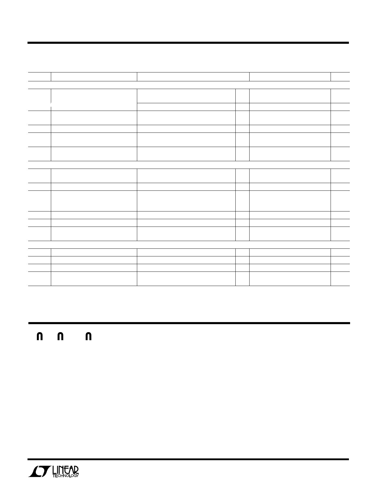
LT1620/LT1621
ELECTRICAL CHARACTERISTICS
IN+ = 16.8V, VCC = 5V, VIOUT = 2V, TA = 25°C unless otherwise noted.
SYMBOL PARAMETER
CONDITIONS
MIN
TYP
MAX
UNITS
Current Sense Amplifier
VOSAVG Input Offset - Measured at ×10 Output VCC ≤ VCM ≤ 32V
(VAVG)
35mV ≤ VID ≤ 125mV
–3
q
–4
VCM = 0V, VID = 80mV
q
– 10
VOSAVG2 Input Offset - Measured at × 20 Output VCC ≤ VCM ≤ 32V
(VAVG2)
0V ≤ VID ≤ 35mV
–3
q
–4
VSENSE No-Load Output Offset
0V ≤ VCM ≤ 32V, VID = 0V, Referenced to VCC q
– 0.1
–3
IB(IN+, IN–) Input Bias Current (Sink)
VCC ≤ VCM ≤ 32V (Note 2)
200
270
q
185
Input Bias Current (Source)
VCM = 0V (Note 2)
4.0
q
Transconductance Amplifier
gm
Amplifier Transconductance
3000
3500
q
2200
AV
Amplifier Voltage Gain
VOLIOUT IOUT Saturation Limit (Sink)
VPROG PROG Input Range
IBPROG Input Bias Current
VOSPROG Input Offset Voltage
(VAVG – VPROG)
End-of-Cycle Comparator
1V ≤ VIOUT ≤ 3V
IIOUT = 50µA
IIOUT = 200µA
IIOUT = 1mA
Measured at PROG Pin
IIOUT = 130µA
60
80
q
0.05
q
0.10
q
0.35
q VCC – 1.25
20
–7
q
–8
VPROG2
VHYST
IBPROG2
VOLMODE
PROG2 Input Range
Input Hysteresis
Input Bias Current
Output Logic Low Output (Sink)
Measured at AVG2 Pin
Measured at PROG2 Pin
IMODE = 0.5mA
IMODE = 10mA
q VCC – 2.5
15
20
q
0.1
q
0.5
3
4
15
3
4
400
430
5.25
5.50
4000
4800
0.15
0.30
0.65
VCC
7
8
VCC – 0.15
0.5
1.2
mV
mV
mV
mV
mV
mV
µA
µA
mA
mA
µmho
µmho
dB
V
V
V
V
nA
mV
mV
V
mV
nA
V
V
The q denotes specifications which apply over the full operating
temperature range.
Note 1: Absolute Maximum Ratings are those values beyond which the
life of a device may be impaired.
Note 2: Input bias currents are disabled when VCC is removed, even
with common mode voltage present at IN+, IN–.
PI FU CTIO S
VCC: 5V ±10% Power Supply Input.
IN+: Sense Amplifier Positive Input. Typically connected
to inductor side of current sense resistor. Common mode
voltage range is 0V to 32V.
IN–: Sense Amplifier Negative Input. Typically connected
to load side of current sense resistor. Common mode
voltage range is 0V to 32V.
SENSE: Sense Amplifier AV = – 1 Output. Used as level-
shifted output for PWM controller current sense input. The
sense output is designed to have an inherent offset to
ensure continuity around zero inductor current. Typical out-
put is –3mV with differential input voltage (IN+ – IN–) = 0.
AVG: Sense Amplifier AV = –10 Output and
Transconductance Amplifier Positive Input. Used as inte-
gration node for average current control. Integration time
constant is calculated using 2.5kΩ typical output imped-
ance.
PROG: Transconductance Amplifier Negative Input. Pro-
gram node for average current delivered to load during
current mode operation. Average current delivered to load
imposes voltage differential at current sense amplifier
3
Share Link: 