VSC7185TW Ver la hoja de datos (PDF) - Vitesse Semiconductor
Número de pieza
componentes Descripción
Fabricante
VSC7185TW Datasheet PDF : 18 Pages
| |||
VITESSE
SEMICONDUCTOR CORPORATION
Preliminary Data Sheet
VSC7185
Quad Transceiver for
Gigabit Ethernet and Fibre Channel
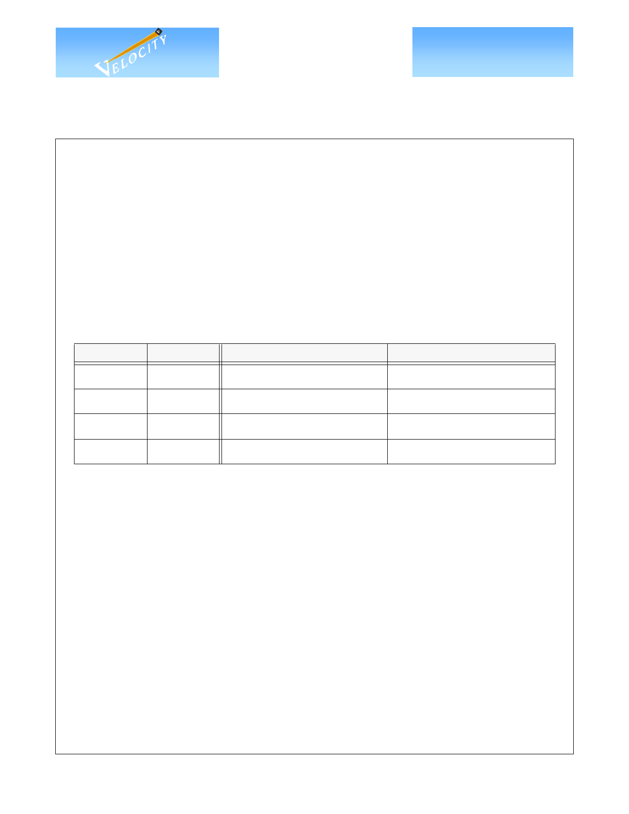
Loopback Operation
Loopback operation is controlled by PLUP (Parallel Loopback) and SLPN (Serial Loopback) as shown in
Table 1. When PLUP=0 and SLPN=1 the part is configured for normal operation. When PLUP=1 and SLPN=1,
SOi is internally looped to SIi and the SOi outputs are held HIGH. When PLUP=0 and SLPN=0, SIi is looped to
SOi after retiming in the clock recovery unit. Although retiming removes much of the input jitter, the SOi out-
puts may not meet jitter specifications listed in the “Transmitter AC Specifications” due to low frequency jitter
transfer from SIi to SOi. When PLUP=1 and SLPN=0 (both loopback paths are active) the clock recovery unit
is used to retime the internally looped SOi data. The SIi inputs are looped directly to the SOi outputs without
retiming. Jitter on SOi in this mode of operation will depend heavily on SIi jitter, and again the SOi outputs may
not meet jitter specifications. The remote receiver will see the total jitter accumulation across both the incoming
and outgoing serial links.
Table 1: Loopback Selection
PLUP
SLPN
LOW
LOW
LOW
HIGH
HIGH
LOW
HIGH
HIGH
Transmitter Source
Receiver
(Retimed)
Transmitter
Receiver
(Not Retimed)
HIGH
Receiver Source
Receiver
Receiver
Transmitter
Transmitter
JTAG Access Port
A JTAG access port is provided to assist in board-level testing. Through this port most pins can be observed
or controlled and all TTL outputs can be tri-stated. A full description of the JTAG functions on this device is
available in “VSC7185 JTAG Access Port Functionality.” Circuits designed exclusively for the HDMP-1685A
will automatically disable the JTAG port. Table 7 (Pinout Definitions) in this datasheet shows the proper con-
nections for either HDMP-1685A emulation or for JTAG functionality (in parentheses).
G52324-0, Rev. 3.0
8/28/00
© VITESSE SEMICONDUCTOR CORPORATION
741 Calle Plano, Camarillo, CA 93012 • 805/388-3700 • FAX: 805/987-5896
Page 5
Share Link: 