VSC7185TW Ver la hoja de datos (PDF) - Vitesse Semiconductor
Número de pieza
componentes Descripción
Fabricante
VSC7185TW Datasheet PDF : 18 Pages
| |||
VITESSE
SEMICONDUCTOR CORPORATION
Quad Transceiver for
Gigabit Ethernet and Fibre Channel
Preliminary Data Sheet
VSC7185
Functional Description
Notation
In this document, each of the four channels are identified as Channel 0, 1, 2 or 3. When discussing a signal
on any specific channel, the signal will have the channel number embedded in the name, for example,
“TX3(0:4).” When referring to the common behavior of a signal which is used on each of the four channels, the
notation “i” is used. Differential signals, i.e. SOi+ and SOi-, may be referred to as a single signal, i.e. SOi, by
dropping reference to the “+” and “-”. RFC refers to the active reference clock input(s), RFCT or RFC+/RFC-.
Clock Synthesizer
To achieve a baud rate clock between 1.05GHz and 1.36GHz, the VSC7185 Clock Multiplier Unit (CMU)
multiplies the reference frequency provided on the RFC input by 10 when RFCM=1, or by 20 when RFCM=0.
The RFCT input is TTL, and the REF+/- inputs are PECL. The on-chip PLL uses a single external 0.1µF capac-
itor, connected between CAP0 and CAP1, to control the Loop Filter. This capacitor should be a multilayer
ceramic dielectric, or better, with at least a 5V working voltage rating and a good temperature coefficient. NPO
is preferred but X7R may be acceptable. These capacitors are used to minimize the impact of common-mode
noise on the Clock Multiplier Unit, especially power supply noise. Higher value capacitors provide better
robustness in systems. NPO is preferred because if an X7R capacitor is used, the power supply noise sensitivity
will vary with temperature.
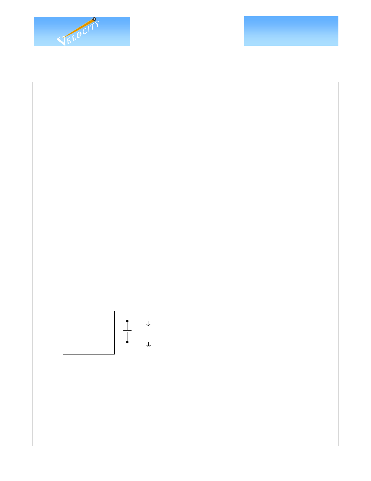
For best noise immunity, the designer may use a three capacitor circuit with one differential capacitor
between CAP0 and CAP1, C1, a capacitor from CAP0 to ground, C2, and a capacitor from CAP1 to ground, C3
(see Figure 1). Larger values are better but 0.1µF is adequate. However, if the designer cannot use a three
capacitor circuit, a single differential capacitor, C1, is adequate. These components should be isolated from
noisy traces.
Figure 1: Loop Filter Capacitors (Best Circuit)
C2
CAP0
VSC7185
C1
CAP1
C3
C1=C2=C3= >0.1uF
MultiLayer Ceramic
Surface Mount
NPO (Preferred) or X7R
5V Working Voltage Rating
Serializer
The VSC7185 accepts 5-bit parallel SSTL-2 input data on the four TXi(0:4) buses along with an SSTL-2
byte clock (TC) and serializes them into four high-speed serial streams. At the source, TXi(0:4) and TC switch
synchronously with respect to an internal 5 bit-time clock. TC and RFC must be derived from the same fre-
quency source so that TC and RFC have a fixed but arbitrary phase relationship when system clocks are stable.
The 5-bit parallel transmission half-characters will be serialized and transmitted on the SOi+/- PECL differen-
tial outputs at the baud rate, with bit TXi0 (10B bit “a” or “i”) transmitted first. User data should be encoded
using 8B/10B or an equivalent code.
Page 2
© VITESSE SEMICONDUCTOR CORPORATION
741 Calle Plano, Camarillo, CA 93012 • 805/388-3700 • FAX: 805/987-5896
G52324-0, Rev. 3.0
8/28/00
Share Link: 