109059790 Ver la hoja de datos (PDF) - Agere -> LSI Corporation
Número de pieza
componentes Descripción
Fabricante
109059790 Datasheet PDF : 50 Pages
| |||
T8535B/T8536B Quad Programmable Codec
Preliminary Data Sheet
September 2001
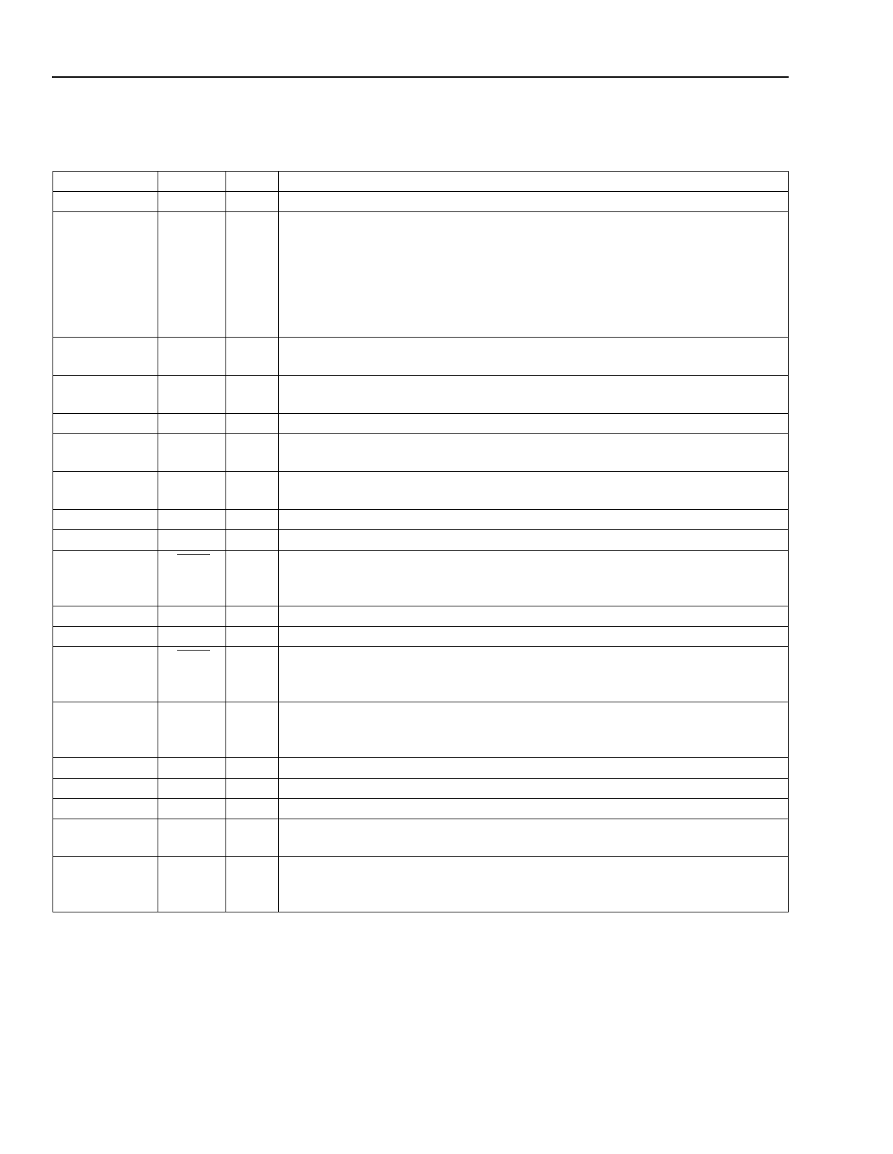
Pin Information (continued)
Table 6. Pin Assignments, 100-Pin TQFP, Common Functions
Pin
1
2, 3, 7—10,
12, 15, 22, 32,
33, 35,
37—40,
44, 50,
59—64, 70,
85, 91—96
4
20, 51, 71, 84
25, 45, 67, 83
68
69
72
73
74
75
76
77
82
86
87
88
89
90
Name
FILTV
NC
SGND
DGND
VDD
FS
BCLK
DX0
DR0
TSX0
DX1
DR1
TSX1
RST
DO
DI
DCLK
CS
INTS
Type
Name/Description
PWR Frequency Synthesizer Power (5 V). This pin must be tied to VDD.
— No Connect. This pin may be used as a tie point.
GND
GND
PWR
I
I
O
I
O
O
I
O
I
O
I
I
I
I
Synthesizer Ground. Connect to digital ground. A common AGND, DGND,
SGND plane is highly recommended.
Digital Ground. Logic ground and return for logic power supply. A common
AGND, DGND, SGND plane is highly recommended.
Digital Power Supply (5 V).
PCM Frame Strobe Input. This 8 kHz clock must be derived from the same
source as BCLK.
PCM Bit Clock Input. This lead is used to develop internal clocks for certain
clock rates.
PCM Transmit Data Output 0. This is a 3-state output.
PCM Receive Data Input 0.
Backplane Line Driver Enable 0 (Active-Low). Normally, these open-drain
outputs are floating in a high-impedance state. When a time slot is active on
DX0, this output pulls low to enable a backplane line driver.
PCM Transmit Data Output 1. This is a 3-state output.
PCM Receive Data Input 1.
Backplane Line Driver Enable 1 (Active-Low). Normally, these open-drain
outputs are floating in a high-impedance state. When a time slot is active on
DX1, this output pulls low to enable a backplane line driver.
Power-On Reset. A low causes a reset of the entire chip. This pin may be
connected to DGND with a 0.1 µF capacitor for a power-on reset function, or it
may be driven by external logic. This lead has an internal pull-up.
Serial Data Output. This is a 3-state output.
Serial Data Input.
Serial Data Clock Input.
Chip Select Input. This lead determines the interval that the serial interface is
active.
Serial Interface Select. Leaving this lead open places the serial interface in
the normal mode; grounding it places the interface into the byte-by-byte mode.
This lead has an internal pull-up.
10
Agere Systems Inc.
Share Link: 