MC1488 Ver la hoja de datos (PDF) - ON Semiconductor
Número de pieza
componentes Descripción
Fabricante
MC1488 Datasheet PDF : 11 Pages
| |||
MC1488
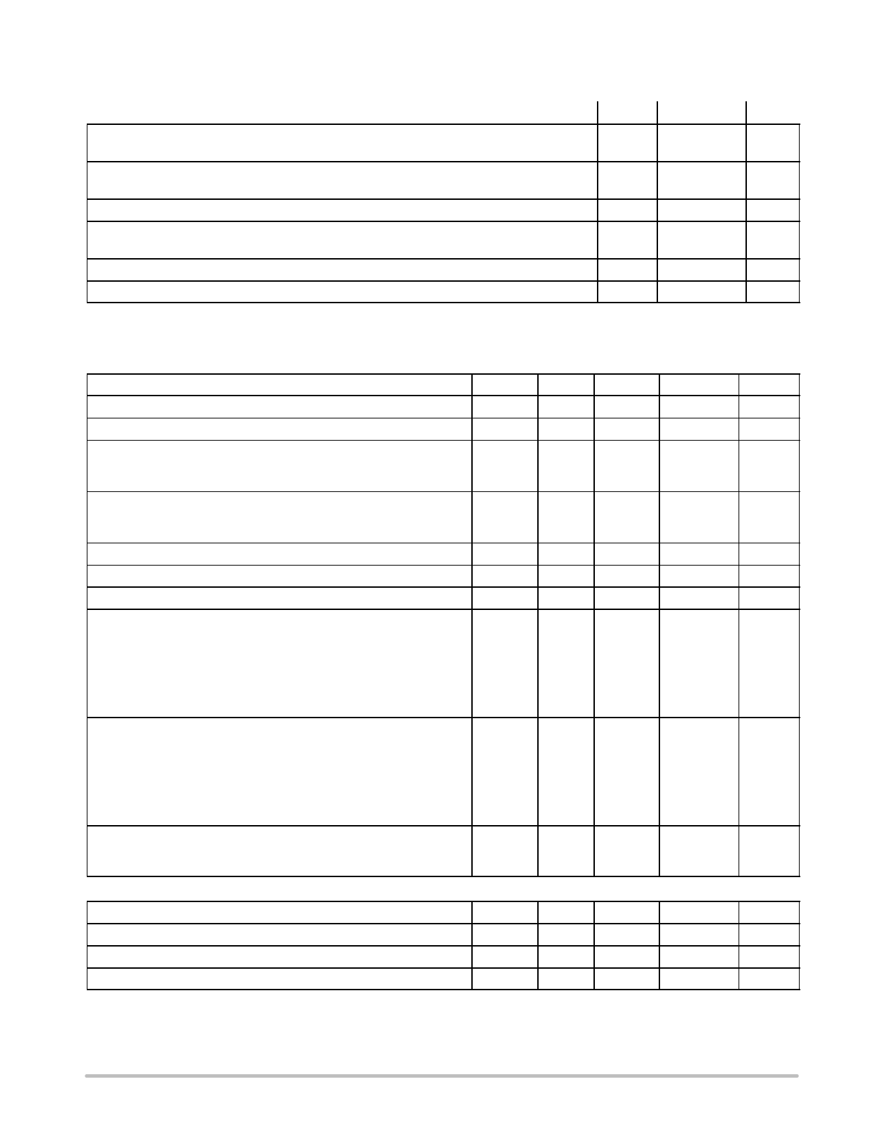
MAXIMUM RATINGS (TA = + 25°C, unless otherwise noted.)
Rating
Symbol
Value
Unit
Power Supply Voltage
Input Voltage Range
VCC
+ 15
Vdc
VEE
− 15
VIR
− 15 p VIR p Vdc
7.0
Output Signal Voltage
VO
± 15
Vdc
Power Derating (Package Limitation, SO−14 and Plastic Dual−In−Line Package)
Derate above TA = + 25°C
PD
1/RqJA
1000
6.7
mW
mW/°C
Operating Ambient Temperature Range
TA
0 to + 75
°C
Storage Temperature Range
Tstg
− 65 to + 175
°C
Stresses exceeding Maximum Ratings may damage the device. Maximum Ratings are stress ratings only. Functional operation above the
Recommended Operating Conditions is not implied. Extended exposure to stresses above the Recommended Operating Conditions may affect
device reliability.
ELECTRICAL CHARACTERISTICS (VCC = + 9.0 ± 1% Vdc, VEE = − 9.0 ± 1% Vdc, TA = 0 to 75°C, unless otherwise noted.)
Characteristic
Symbol
Min
Typ
Max
Unit
Input Current − Low Logic State (VIL = 0)
Input Current − High Logic State (VIH = 5.0 V)
Output Voltage − High Logic State
(VIL = 0.8 Vdc, RL = 3.0 kW , VCC = + 9.0 Vdc, VEE = − 9.0 Vdc)
(VIL = 0.8 Vdc, RL = 3.0 kW , VCC = + 13.2 Vdc, VEE = − 13.2 Vdc)
Output Voltage − Low Logic State
(VIH = 1.9 Vdc, RL = 3.0 kW , VCC = + 9.0 Vdc, VEE = − 9.0 Vdc)
(VIH = 1.9 Vdc, RL = 3.0 kW , VCC = + 13.2 Vdc, VEE = − 13.2 Vdc)
Positive Output Short−Circuit Current, Note 1
Negative Output Short−Circuit Current, Note 1
Output Resistance (VCC = VEE = 0, ⎥ VO ⎜ = ± 2.0 V)
Positive Supply Current (RI = ∞)
(VIH = 1.9 Vdc, VCC = + 9.0 Vdc)
(VIL = 0.8 Vdc, VCC = + 9.0 Vdc)
(VIH = 1.9 Vdc, VCC = + 12 Vdc)
(VIL = 0.8 Vdc, VCC = + 12 Vdc)
(VIH = 1.9 Vdc, VCC = + 15 Vdc)
(VIL = 0.8 Vdc, VCC = + 15 Vdc)
Negative Supply Current (RL = ∞)
(VIH = 1.9 Vdc, VEE = − 9.0 Vdc)
(VIL = 0.8 Vdc, VEE = − 9.0 Vdc)
(VIH = 1.9 Vdc, VEE = − 12 Vdc)
(VIL = 0.8 Vdc, VEE = − 12 Vdc)
(VIH = 1.9 Vdc, VEE = − 15 Vdc)
(VIL = 0.8 Vdc, VEE = − 15 Vdc)
Power Consumption
(VCC = 9.0 Vdc, VEE = − 9.0 Vdc)
(VCC = 12 Vdc, VEE = − 12 Vdc)
IIL
IIH
VOH
VOL
IOS +
IOS −
ro
ICC
IEE
PC
−
−
+ 6.0
+ 9.0
− 6.0
− 9.0
+ 6.0
− 6.0
300
−
−
−
−
−
−
−
−
−
−
−
−
−
−
1.0
−
+ 7.0
+ 10.5
− 7.0
− 10.5
+ 10
− 10
−
+ 15
+ 4.5
+ 19
+ 5.5
−
−
− 13
−
− 18
−
−
−
−
−
1.6
10
−
−
−
−
+ 12
− 12
−
+ 20
+ 6.0
+ 25
+ 7.0
+ 34
+ 12
− 17
− 500
− 23
− 500
− 34
− 2.5
333
576
mA
mA
Vdc
Vdc
mA
mA
Ohms
mA
mA
mA
mA
mA
mA
mA
mW
SWITCHING CHARACTERISTICS (VCC = + 9.0 ± 1% Vdc, VEE = − 9.0 ± 1% Vdc, TA = + 25°C.)
Propagation Delay Time (zI = 3.0 k and 15 pF)
tPLH
−
275
350
ns
Fall Time
(zI = 3.0 k and 15 pF)
tTHL
−
45
75
ns
Propagation Delay Time (zI = 3.0 k and 15 pF)
tPHL
−
110
175
ns
Rise Time
(zI = 3.0 k and 15 pF)
tTLH
−
55
100
ns
1. Maximum Package Power Dissipation may be exceeded if all outputs are shorted simultaneously.
http://onsemi.com
3
Share Link: 