MC10H352FN Ver la hoja de datos (PDF) - Motorola => Freescale
Número de pieza
componentes Descripción
Fabricante
MC10H352FN Datasheet PDF : 4 Pages
| |||
MOTOROLA
SEMICONDUCTOR TECHNICAL DATA
Quad CMOS to PECL*
Translator
MC10H352
The MC10H352 is a quad translator for interfacing data between a
CMOS logic section and the PECL section of digital systems when only a
+5.0 Vdc power supply is available. The MC10H352 has CMOS
compatible inputs and PECL complementary open–emitter outputs that
allow use as an inverting/non–inverting translator or as a differential line
driver. When the common strobe input is at a low logic level, it forces all
true outputs to the PECL low logic state (≈ +3.2 V) and all inverting
outputs to the PECL high logic state (≈ +4.1 V).
The MC10H352 can also be used with the MC10H350 to transmit and
receive CMOS information differentially via balanced twisted pair lines.
• Single +5.0 V Power Supply
• All VCC Pins Isolated On Chip
• Differentially Drive Balanced Lines
• tpd = 1.3 nsec Typical
MAXIMUM RATINGS
Characteristic
Power Supply
Input Voltage (VCC = 5.0 V)
Output Current — Continuous
— Surge
Symbol
Rating
Unit
VCC
VI
Iout
0 to +7.0
Vdc
0 to VCC
Vdc
50
mA
100
Operating Temperature Range
Storage Temperature Range — Plastic
— Ceramic
TA
0 to +75
°C
Tstg
–55 to +150
°C
–55 to +165
ELECTRICAL CHARACTERISTICS (VCC = VCC1 = VCC2 = 5.0 V ± 5.0%)
0°
25°
75°
Characteristic
Symbol Min Max Min Max Min Max Unit
Power Supply
Current
ECL
— 50 — 45 —
50 mA
TTL
— 20 — 15 —
20 mA
Reverse Current
Pins 7, 8, 12, 14
Pin 9
IR
µA
— 25 — 20 —
25
— 100 — 80 — 100
Forward Current
Pins 7, 8, 12, 14
Pin 9
IF
mA
— –0.8 — –0.6 — –0.8
— –3.2 — –2.4 — –3.2
Input Voltage
Breakdown
V(BR)in 5.5 — 5.5 — 5.5
— Vdc
Input Clamp Voltage
(Iin = –18 mA)
High Output
Voltage (1)
VI
— –1.5 — –1.5 — –1.5 Vdc
VOH 3.98 4.16 4.02 4.19 4.08 4.27 Vdc
Low Output
Voltage (1)
VOL 3.05 3.37 3.05 3.37 3.05 3.37 Vdc
High Input Voltage
Low Input Voltage
VIH 3.15 — 3.15 — 3.15 — Vdc
VIL
— 1.5 — 1.5 —
1.5 Vdc
(1) With VCC at 5.0 V. VOH/VOL change 1:1 with VCC.
*Positive Emitter Coupled Logic
L SUFFIX
CERAMIC PACKAGE
CASE 732–03
P SUFFIX
PLASTIC PACKAGE
CASE 738–03
FN SUFFIX
PLCC
CASE 775–02
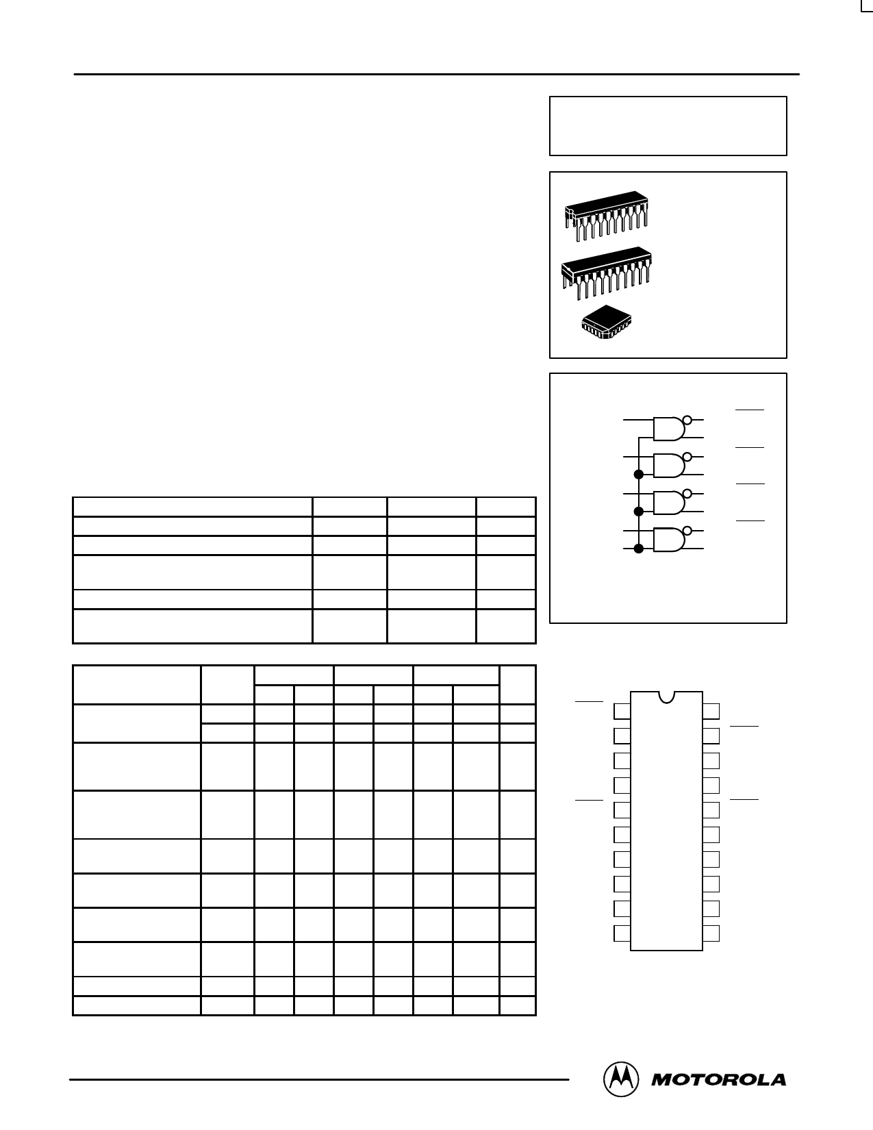
LOGIC DIAGRAM
B IN 7
A IN 8
D IN 12
C IN 14
COMMON 9
STROBE
1 B OUT
2 B OUT
5 A OUT
4 A OUT
16 D OUT
17 D OUT
19 C OUT
18 C OUT
VCC (+5.0 VDC) = PINS 6, 11, 15, 20
GND = PIN 10
DIP
PIN ASSIGNMENT
B OUT
1
B OUT
2
20
ECL VCC
19
C OUT
N.C.
3
18
C OUT
A OUT
4
17
D OUT
A OUT
5
16
D OUT
VCC
6
B IN
7
15
VCC 2
14
C IN
A IN
8
13
N.C.
COMMON
STROBE
9
12
D IN
GND
10
11
CMOS VCC
Pin assignment is for Dual–in–Line Package.
For PLCC pin assignment, see the Pin Conversion
Tables on page 6–36 of the Motorola MECL Data
Book (DL122/D).
3/93
© Motorola, Inc. 1996
2–96
REV 5
Share Link: 