LC4608C Ver la hoja de datos (PDF) - SANYO -> Panasonic
Número de pieza
componentes Descripción
Fabricante
LC4608C Datasheet PDF : 11 Pages
| |||
LC4608C
Continued from preceding page.
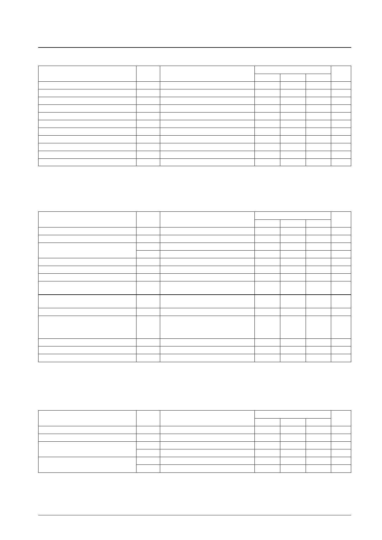
Parameter
Symbol
Conditions
Ratings
Unit
min
typ
max
STBCLK frequency
CLK → LOAD setup time
LOAD → CLK hold time
LOAD pulse width
STBCLK → LOAD setup time
LOAD → STBCLK hold time
Clock rising edge time
Clock falling edge time
Latch rising edge time
Latch falling edge time
Operating temperature
fSTB
tSL
tHL
tWL
tSTBL
tLSTB
tr
tf
tlr
tlf
Tjopr
1.0 MHz
80
ns
80
ns
80
ns
80
ns
80
ns
35
ns
35
ns
70
ns
70
ns
–1.0
+90
°C
Note : 1. The figures for normal operation are a load capacitance Cpzt of 1 nF, a power supply voltage VH of 30 V, and a max input level COMmax of 25 V.
2. Value for VH = 40 V, COMmax = 40 V, frequency = 35 kHz, and duty factor = 1/100.
Electrical Characteristics
DC Characteristics at VDD = 5.0 V±10%, Tjopr = –10 to +90°C unless otherwise specified
Parameter
Input high-level voltage
Input low-level voltage
Input high-level current *2
Input low-level current *3
Output high- level voltage
Output low-level voltage
Output high-level current transmission gate
voltage
Output low-level current transmission gate
voltage
Transmission gate on resistance
Transmission gate on resistance variation
Symbol
Conditions
VIH
VIL
–IIH1
–IIH2
IIL
VOH
VOL
VOHT
VOLT
RON
Rx
VDD = 5.0 V, VIH = 5.0 V
VDD = 5.0 V, VIH = 5.0 V
VDD = 5.0 V
IO = –400 µA
IO = 400 µA
VDD = 5.0 V, VH = 40 V, COMn = 40 V,
IOHT = 10 mA
VDD = 5.0 V, VH = 40 V, COMn = 40 V,
–IOHT = 10 mA
VH = 40 V, VDS = 3 V
Within chip
2 (MAX – MIN) × 100
——————————
MAX + MIN
Ratings
Unit
min
typ
max
VDD × 0.7
–0.3
0
VDD +0.3 V
VDD × 0.3 V
0.5 µA
0
50
100 µA
0
0.5 µA
VDD – 0.5
V
0.5 V
39
39.4
V
0.6
1.0 V
60
100 Ω
–15
+15 Ω
Current drain
Leakage current between pins
IDD1 VDD – GND, fclk = 3.5 MHz, fSln = 1.75 MHz
–15
±INL Leakage current between pins
0
+15 Ω
10 µA
Output leakage current
ILEAK VDD = 5.0 V, VH = 42 V
0
100 µA
Note : 1. The sign is negative for incoming current and positive for outgoing current.
2. –IIH1 applies to the following input pins: SI0 to SI3, CLK, LAT, LOAD, STBCLK, and STB1 to STB3. –IIH applies to the following input pins: STB4
and STB5.
3. IIL1 applies to the following input pins: SI0 to SI3, CLK, LAT, LOAD, STBCLK, and STB1 to STB5.
Switching Characteristics at VDD = 5.0 V±10%, Tjopr = –10 to +90°C unless otherwise specified
Parameter
Symbol
Conditions
Ratings
Unit
min
typ
max
SOn output rising edge time
SOn input rising edge time
STBn → DOn propagation delay time
tor
CL = 10 pF
tof
CL = 10 pF
tdor
*5
tdof
*5
50
ns
50
ns
1.0
µs
1.0
µs
CLK → SOn propagation delay time
tsor
CL = 10 pF
tsof
CL = 10 pF
140
ns
140
ns
Note : 5. The figures are for a load capacitance Cpzt of 1 nF and a power supply voltage VH of 30 V as measured with RL = 3 kΩ and COMn = 25 V DC.
No. 5782-2/11
Share Link: 