ICL7109 Ver la hoja de datos (PDF) - Intersil
Número de pieza
componentes Descripción
Fabricante
ICL7109 Datasheet PDF : 25 Pages
| |||
ICL7109
De-Integrate Phase
The final phase is de-integrate, or reference integrate. Input
low is internally connected to analog COMMON and input
high is connected across the previously charged (during
auto-zero) reference capacitor. Circuitry within the chip
ensures that the capacitor will be connected with the correct
polarity to cause the integrator output to return to zero cross-
ing (established in Auto-Zero) with a fixed slope. The time
required for the output to return to zero is proportional to the
input signal.
Differential Input
The input can accept differential voltages anywhere within the
common mode range of the input amplifier, or specifically from
1V below the positive supply to 1.5V above the negative sup-
ply. In this range, the system has a CMRR of 86dB typical.
However, care must be exercised to assure the integrator out-
put does not saturate. A worst case condition would be a large
positive common mode voltage with a near full-scale negative
differential input voltage. The negative input signal drives the
integrator positive when most of its swing has been used up
by the positive common mode voltage. For these critical appli-
cations the integrator output swing can be reduced to less
than the recommended 4V full scale swing with little loss of
accuracy. The integrator output can swing to within 0.3V of
either supply without loss of linearity.
CREF
RINT
CREF+
37
REF IN+
36
A-Z
35
IN HI
INT
DE-
REF IN- CREF -
39
38
BUFFER
30
A-Z
-
+
BUFFER
DE+
A-Z
33
COMMON
IN LO
34
INT
DE+
DE-
A-Z
DE(±)
CAZ
A-Z
31
-
+
INTEGRATOR
CINT
INT
32
COMPARATOR
TO ZERO CROSS
+
DETECTOR
DIGITAL SECTION
A-Z
10µA
-
+
6.2V
AZ
INT
DE+
DE-
FROM CONTROL
LOGIC
DIGITAL SECTION
29
REF OUT
28
40
V-
V+
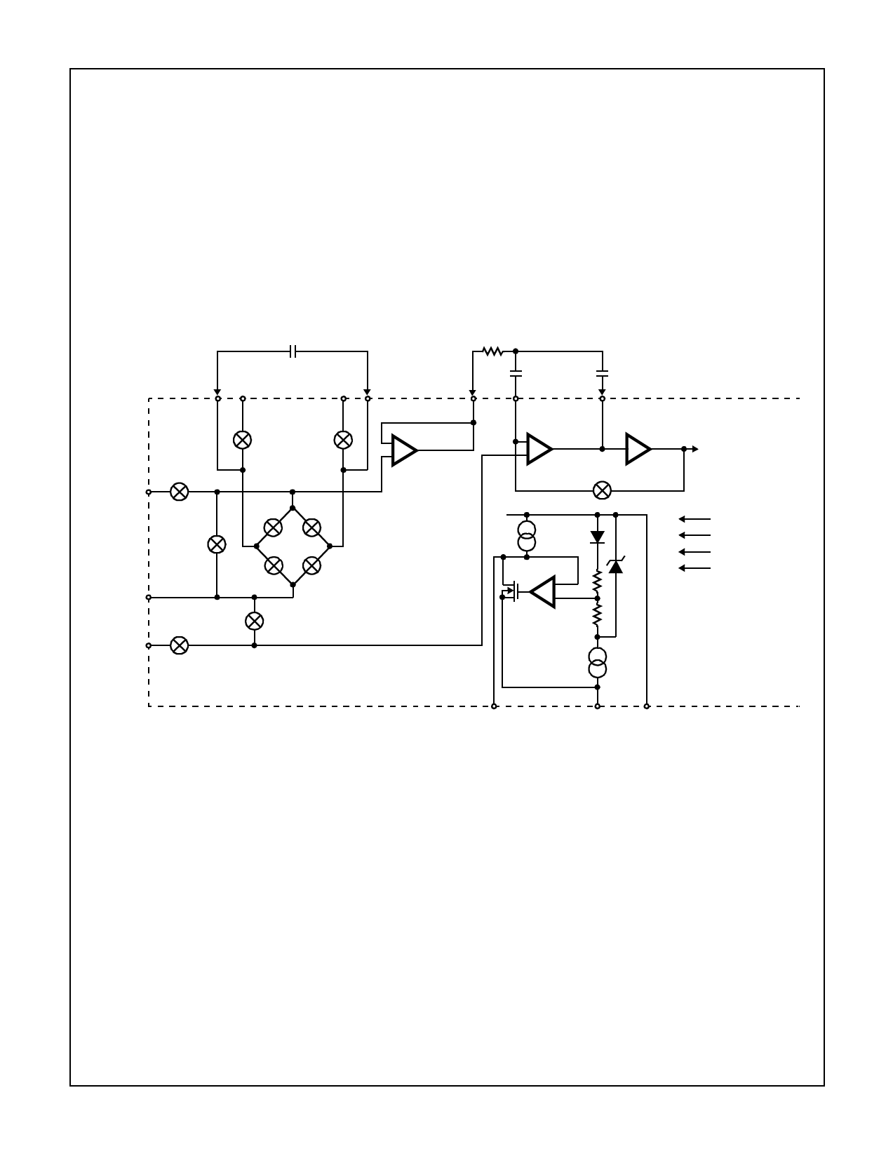
FIGURE 2. ANALOG SECTION OF ICL7109
The ICL7109 has, however, been optimized for operation
with analog common near digital ground. With power sup-
plies of +5V and -5V, this allows a 4V full scale integrator
swing positive or negative thus maximizing the performance
of the analog section.
Differential Reference
The reference voltage can be generated anywhere within the
power supply voltage of the converter. The main source of
common mode error is a roll-over voltage caused by the
reference capacitor losing or gaining charge to stray capacity
on its nodes. If there is a large common mode voltage, the ref-
erence capacitor can gain charge (increase voltage) when
called up to deintegrate a positive signal but lose charge
(decrease voltage) when called up to deintegrate a negative
input signal. This difference in reference for positive or
negative input voltage will give a roll-over error. However, by
selecting the reference capacitor large enough in comparison
to the stray capacitance, this error can be held to less than 0.5
count worst case. (See Component Value Selection.)
The roll-over error from these sources is minimized by having
the reference common mode voltage near or at analog
COMMON.
Component Value Selection
For optimum performance of the analog section, care must
be taken in the selection of values for the integrator capaci-
tor and resistor, auto-zero capacitor, reference voltage, and
conversion rate. These values must be chosen to suit the
particular application.
The most important consideration is that the integrator out-
put swing (for full-scale input) be as large as possible. For
example, with ±5V supplies and COMMON connected to
Teflon™ is a trademark of DuPont Corporation
9
Share Link: 