ICL7109 Ver la hoja de datos (PDF) - Intersil
Número de pieza
componentes Descripción
Fabricante
ICL7109 Datasheet PDF : 25 Pages
| |||
ICL7109
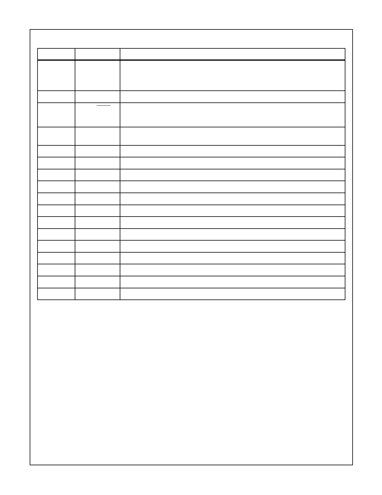
Pin Descriptions (Continued)
PIN
SYMBOL
DESCRIPTION
24
OSC SEL
Oscillator Select - Input high configures OSC IN, OSC OUT, BUF OSC OUT as RC oscillator - clock
will be same phase and duty cycle as BUF OSC OUT.
Input low configures OSC IN, OSC OUT for crystal oscillator - clock frequency will be 1/58 of
frequency at BUF OSC OUT.
25
BUF OSC OUT Buffered Oscillator Output
26
RUN/HOLD
Input High - Conversions continuously performed every 8192 clock pulses.
Input Low - Conversion in progress completed, converter will stop in Auto-Zero 7 counts before
integrate.
27
SEND
Input - Used in handshake mode to indicate ability of an external device to accept data. Connect to
+5V if not used.
28
V-
Analog Negative Supply - Nominally -5V with respect to GND (Pin 1).
29
REF OUT
Reference Voltage Output - Nominally 2.8V down from V+ (Pin 40).
30
BUFFER
Buffer Amplifier Output.
31
AUTO-ZERO Auto-Zero Node - Inside foil of CAZ .
32
INTEGRATOR Integrator Output - Outside foil of CINT.
33
COMMON
Analog Common - System is Auto-Zeroed to COMMON.
34
INPUT LO
Differential Input Low Side.
35
INPUT HI
Differential Input High Side.
36
REF IN +
Differential Reference Input Positive.
37
REF CAP +
Reference Capacitor Positive.
38
REF CAP-
Reference Capacitor Negative.
39
REF IN-
Differential Reference Input Negative.
40
V+
Positive Supply Voltage - Nominally +5V with respect to GND (Pin 1).
NOTE: All digital levels are positive true.
5
Share Link: 