ICL7109 Ver la hoja de datos (PDF) - Intersil
Número de pieza
componentes Descripción
Fabricante
ICL7109 Datasheet PDF : 25 Pages
| |||
ICL7109
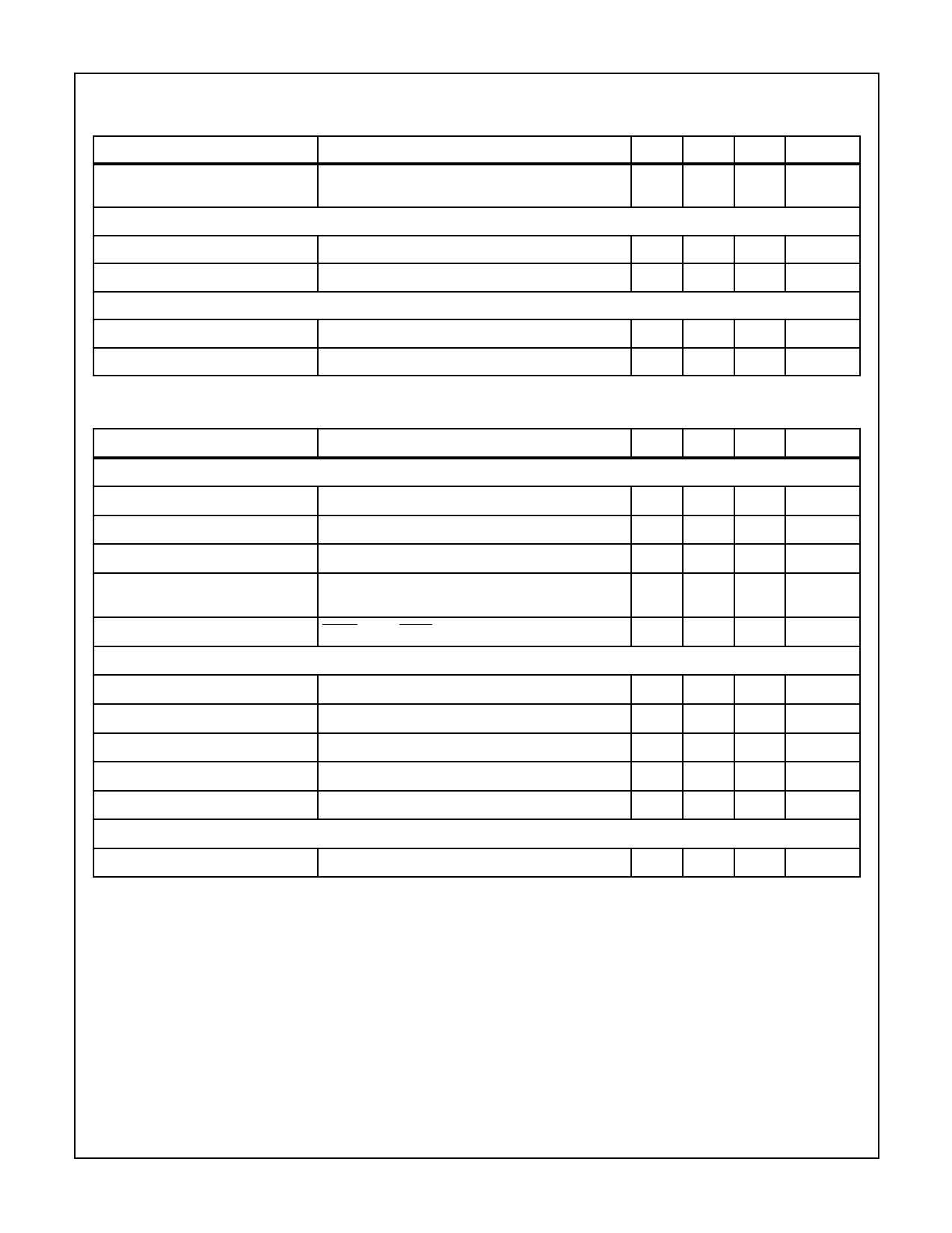
Analog Electrical Specifications V+ = +5V, V- = -5V, GND = 0V, TA = 25oC, fCLK = 3.58MHz,
Unless Otherwise Specified (Continued)
PARAMETER
TEST CONDITIONS
MIN TYP MAX
UNIT
Scale Factor Temperature Coefficient VIN = 408.9mV = > 77708 Reading Ext. Ref. 0ppm/oC
-
1
5
ppm/oC
(Note 4)
REFERENCE VOLTAGE
Ref Out Voltage, VREF
Ref Out Temperature Coefficient
Referred to V+, 25kΩ Between V+ and REF OUT
25kΩ Between V+ and REF OUT (Note 4)
-2.4 -2.8 -3.2
V
-
80
-
ppm/oC
POWER SUPPLY CHARACTERISTICS
Supply Current V+ to GND, I+
Supply Current V+ to V-, ISUPP
VIN = 0V, Crystal Osc 3.58MHz Test Circuit
Pins 2 - 21, 25, 26, 27, 29; Open
-
700 1500
µA
-
700 1500
µA
Digital Electrical Specifications V+ = +5V, V- = -5V, GND = 0V, TA = 25oC, Unless Otherwise Specified
PARAMETER
TEST CONDITIONS
MIN TYP MAX
UNIT
DIGITAL OUTPUTS
Output High Voltage, VOH
Output Low Voltage, VOL
Output Leakage Current
IOUT = 100µA Pins 2 - 16, 18, 19, 20
IOUT = 1.6mA Pins 2 - 16, 18, 19, 20
Pins 3 - 16 High Impedance
3.5
4.3
-
V
-
±0.20 ±0.40
V
-
±0.01 ±1
µA
Control I/O Pullup Current
Pins 18, 19, 20 VOUT = V+ -3V MODE Input at GND
-
5
-
µA
(Note 4)
Control I/O Loading
HBEN Pin 19 LBEN Pin 18 (Note 4)
-
−
50
pF
DIGITAL INPUTS
Input High Voltage, VIH
Input Low Voltage, VIL
Input Pull-Up Current
Input Pull-Up Current
Input Pull-Down Current
TIMING CHARACTERISTICS
Pins 18 - 21, 26, 27 Referred to GND
Pins 18 - 21, 26, 27 Referred to GND
Pins 26, 27 VOUT = (V+) -3V
Pins 17, 24 VOUT = (V+) -3V
Pin 21 VOUT = GND +3V
3.0
-
-
V
-
-
1
V
-
5
-
µA
-
25
-
µA
-
5
-
µA
MODE Input Pulse Width, tW
(Note 4)
50
-
-
ns
NOTES:
1. Input voltages may exceed the supply voltages provided the input current is limited to ±100µA.
2. Due to the SCR structure inherent in the process used to fabricate these devices, connecting any digital inputs or outputs to voltages
greater than V+ or less than GND may cause destructive device latchup. For this reason it is recommended that no inputs from sources
other than the same power supply be applied to the ICL7109 before its power supply is established, and that in multiple supply systems
the supply to the ICL7109 be activated first.
3. This limit refers to that of the package and will not be obtained during normal operation.
4. This parameter is not production tested, but is guaranteed by design.
5. Roll-over error for TA = -55oC to 125oC is ±10 counts (Max).
6. A full scale voltage of 2.048V is used because a full scale voltage of 4.096V exceeds the devices Common Mode Voltage Range.
7. For CERDIP package the Ratiometric error can be -4 (Min).
3
Share Link: 