ICL7109 Ver la hoja de datos (PDF) - Intersil
Número de pieza
componentes Descripción
Fabricante
ICL7109 Datasheet PDF : 25 Pages
| |||
ICL7109
Absolute Maximum Ratings
Positive Supply Voltage (GND to V+). . . . . . . . . . . . . . . . . . . . +6.0V
Negative Supply Voltage (GND to V-) . . . . . . . . . . . . . . . . . . . . . -9V
Analog Input Voltage (Either Input) (Note 1) . . . . . . . . . . . . V+ to V-
Reference Input Voltage (Either Input) (Note 1) . . . . . . . . . . V+ to V-
Digital Input Voltage . . . . . . . . . . . . . . . . . . . . . . . . . . . . . (V+) +0.3V
Pins 2-27 (Note 2) . . . . . . . . . . . . . . . . . . . . . . . . . . . . . . GND -0.3V
Operating Conditions
Temperature Range
M Suffix . . . . . . . . . . . . . . . . . . . . . . . . . . . . . . . . . -55oC to 125oC
I Suffix . . . . . . . . . . . . . . . . . . . . . . . . . . . . . . . . . . . -25oC to 85oC
C Suffix . . . . . . . . . . . . . . . . . . . . . . . . . . . . . . . . . . . .0oC to 75oC
Thermal Information
Thermal Resistance (Typical, Note 1)
θJA (oC/W) θJC (oC/W)
SBDIP Package. . . . . . . . . . . . . . . . . . . .
60
20
CERDIP Package . . . . . . . . . . . . . . . . . .
55
18
PDIP Package . . . . . . . . . . . . . . . . . . . . .
50
N/A
Maximum Junction Temperature (PDIP Package) . . . . . . . . . 150oC
Maximum Junction Temperature (CERDIP Package). . . . . . . 175oC
Maximum Storage Temperature Range . . . . . . . . . . -65oC to 150oC
Maximum Lead Temperature (Soldering 10s Max). . . . . . . . . 300oC
CAUTION: Stresses above those listed in “Absolute Maximum Ratings” may cause permanent damage to the device. This is a stress only rating and operation
of the device at these or any other conditions above those indicated in the operational sections of this specification is not implied.
NOTE:
1. θJA is measured with the component mounted on an evaluation PC board in free air.
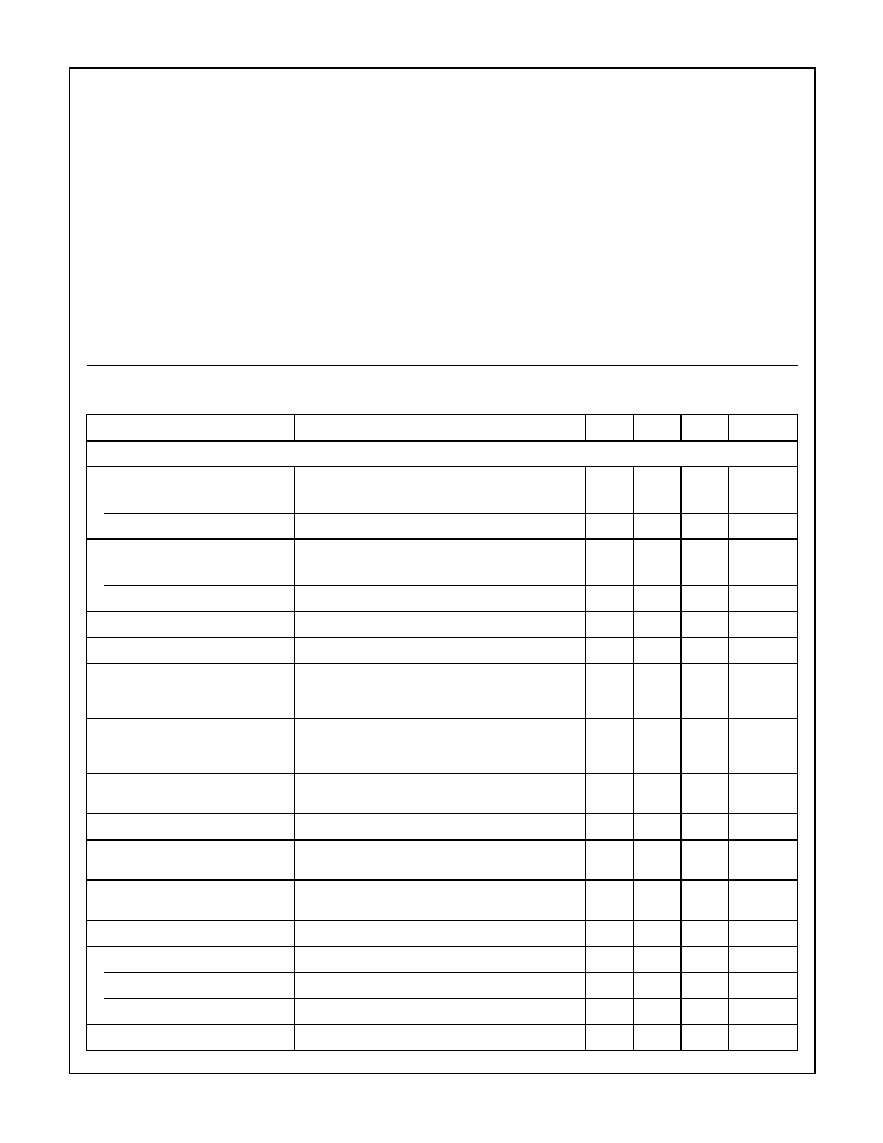
Analog Electrical Specifications V+ = +5V, V- = -5V, GND = 0V, TA = 25oC, fCLK = 3.58MHz,
Unless Otherwise Specified
PARAMETER
TEST CONDITIONS
SYSTEM PERFORMANCE
Oscillator Output Current
High, OOH
Low, OOL
Buffered Oscillator Output Current
High, BOOH
Low, BOOL
Zero Input Reading
Ratiometric Error
Non-Linearity
VOUT = 2.5V
VOUT = 2.5V
VOUT = 2.5V
VOUT = 2.5V
VIN = 0.0000V, VREF = 204.8mV
VlN = VREF, VREF = 204.8mV (Note 7)
Full Scale = 409.6mV to 2.048mV
Maximum Deviation from Best Straight Line Fit, Over
Full Operating Temperature Range (Notes 4 and 6)
Rollover Error
Linearity
Full Scale = 409.6mV to 2.048V
Difference in Reading for Equal Positive and Negative
Inputs Near Full Scale (Notes 5 and 6), R1 = 0Ω
Full-Scale = 200mV or Full Scale = 2V Maximum
Deviation from Best Straight Line Fit (Note 4)
Common Mode Rejection Ratio, CMRR VCM = ±1V, VIN = 0V, Full Scale = 409.6mV
Input Common Mode Range, VCMR Input HI, Input LO, Common (Note 4)
Noise, eN
Leakage Current Input, IILK
ICL7109CPL
ICL7109IDL
ICL7109MDL
Zero Reading Drift
VIN = 0V, Full-Scale = 409.6mV
(Peak-to-Peak Value Not Exceeded 95% of Time)
VlN = 0V, All Devices at 25oC (Note 4)
0oC to 70oC (Note 4)
-25oC to 85oC (Note 4)
-55oC to 125oC
VlN = 0V, R1 - 0Ω (Note 4)
MIN TYP MAX
-
1
-
-
1.5
-
-
2
-
-
5
-
-0000 ±0000 +0000
-3
-
0
-1
±0.2
+1
-1
±0.2
+1
-
±0.2
±1
-
50
-
(V-)
-
(V+)
+2.0
-2.0
-
15
-
-
1
10
-
20
100
-
100 250
-
2
100
-
0.2
1
UNIT
mA
mA
mA
mA
Counts
Counts
Counts
Counts
Counts
µV/V
V
µV
pA
pA
pA
nA
µV/oC
2
Share Link: 