ML4812 Ver la hoja de datos (PDF) - Fairchild Semiconductor
Número de pieza
componentes Descripción
Fabricante
ML4812 Datasheet PDF : 16 Pages
| |||
ML4812
FUNCTIONAL DESCRIPTION (Continued)
OUTPUT DRIVER STAGE
The ML4812 output driver is a 1A peak output high speed
totem pole circuit designed to quickly drive capacitive
loads, such as power MOSFET gates. (Figure 3)
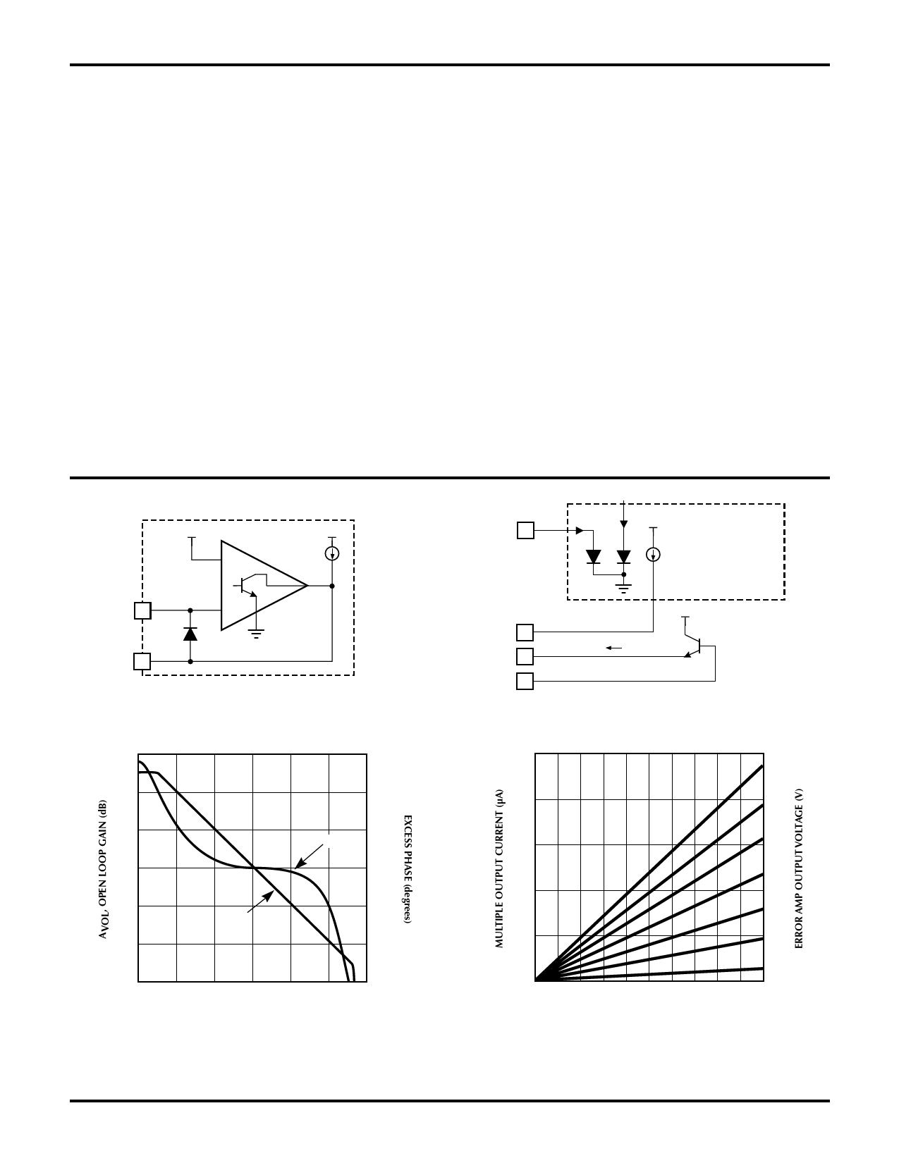
ERROR AMPLIFIER
The ML4812 error amplifier is a high open loop gain,
wide bandwidth, amplifier.(Figures 4-5)
GAIN MODULATOR
The ML4812 gain modulator is of the current-input type
to provide high immunity to the disturbances caused by
high power switching. The rectified line input sine wave is
converted to a current via a dropping resistor. In this way,
small amounts of ground noise produce an insignificant
effect on the reference to the PWM comparator. The
output of the gain modulator is a current of the form: IOUT
is proportional to ISINE ↔ IEA, where ISINE is the current in
the dropping resistor, and IEA is a current proportional to
5V
+
EA–
4
–
EA OUT
3
8V
0.5mA
Figure 4. Error Amplifier Configuration
the output of the error amplifier. When the error amplifier
is saturated high, the output of the gain modulator is
approximately equal to the ISINE input current. The gain
modulator output current is converted into the reference
voltage for the PWM comparator through a resistor to
ground on the gain modulator output. The gain modulator
output is clamped to 5V to provide current limiting.
Ramp compensation is accomplished by subtracting 1/2
of the current flowing out of RAMP COMP through a
buffer transistor driven by CT which is set by an external
resistor.
UNDER VOLTAGE LOCKOUT
On power-up the ML4812 remains in the UVLO
condition; output low and quiescent current low. The IC
becomes operational when VCC reaches 16V. When VCC
drops below 10V, the UVLO condition is imposed.
During the UVLO condition, the 5V VREF pin is “off”,
making it usable as a “flag” for starting up a downstream
PWM converter.
ISINE
6
ERROR CURRENT
9V
ISINE × ERROR CURRENT
– IRAMP COMP/2
GM OUT
2
RAMP COMP
7
CT
16
5V
IRAMP COMP
Figure 6. Gain Modulator Block Diagram
100
0
80
-30
60
-60
PHASE
40
-90
20
GAIN
0
-120
-150
-20
-180
10 100 1k 10k 100k 1M 10M
FREQUENCY (Hz)
500
400
300
200
100
0
0
4.5
4.0
3.5
3.0
100
200
300
400
SINE INPUT CURRENT (µA)
2.5
2.0
1.5
500
Figure 5. Error Amplifier Open-Loop Gain and
Phase vs Frequency
6
Figure 7. Gain Modulator Linearity
REV. 1.0 10/10/2000
Share Link: 