LA4533M Ver la hoja de datos (PDF) - SANYO -> Panasonic
Número de pieza
componentes Descripción
Fabricante
LA4533M Datasheet PDF : 3 Pages
| |||
LA4533M
Continued from preceding page.
Parameter
Total harmonic distortion
Output power
Crosstalk
Ripple rejection
Output noise voltage
Power off effect
Muting effect
Power on current sensitivity
Power off voltage sensitivity
Muting off current sensitivity
Muting on voltage sensitivity
Symbol
Conditions
THD
PO
CT
SVRR
VNO
VO (off)
VO (MT)
I1 (on)
V1 (off)
I10 (off)
V10 (on)
VCC=2.0V, f=1kHz, PO=1mW
VCC=3.0V, f=1kHz, THD=10%
VCC=2.4V, f=100Hz, Rg=1kΩ, VO=–10dB
VCC=1.6V, f=100Hz, Rg=1kΩ, VR=–20dBm,
BPF=100Hz
VCC=4.5V, Rg=1kΩ, BPF=20Hz to 20kHz
VCC=1.6V, f=100Hz, pin 1 → GND, VIN=–10dB
VCC=1.6V, f=100Hz, pin 10 → GND, VIN=–10dB
VCC=1.5V, V5 ≥ 0.85V
VCC=1.5V, V5 ≤ 0.1V
VCC=1.5V, V5 ≥ 0.85V
VCC=1.5V, V5 ≤ 0.1V
Ratings
Unit
min
typ
max
0.5
1.5 %
20
40
mW
40
50
dB
45
60
dB
62
0.05
0.5
0.6
0.2
0.5 0.65
100 µV
–80 dB
–80 dB
1.0 µA
V
1.0 µA
V
Note) The quiescent current is represented by the current flowing into pin 6. The respective maximum currents flowing
into pin 1 and pin 10 are calculated by (pin voltage –0.5) / 16 [V/kΩ] and the total current increases by these
current values.
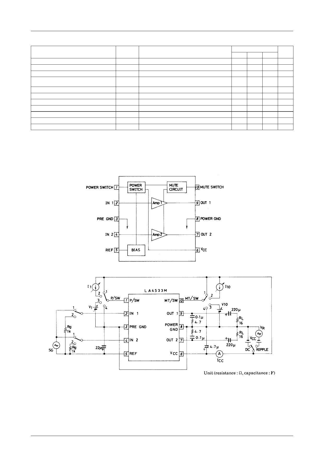
Equivalent Circuit Block Diagram and Application Circuit
Test Circuit
No.2248–2/3
Share Link: 