LB1875 Ver la hoja de datos (PDF) - SANYO -> Panasonic
Número de pieza
componentes Descripción
Fabricante
LB1875 Datasheet PDF : 17 Pages
| |||
LB1875
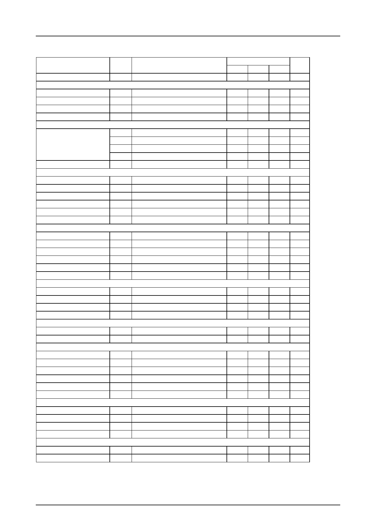
Electrical Characteristics at Ta = 25°C, VCC = 12V
Parameter
Symbol
Conditions
Power supply current
[5V regulated output ]
Output fluctuation
Voltage fluctuation
Load fluctuation
Temperature coefficcient
[Output Section]
Output saturation voltage
Output leak current
[Hall amplifier]
Input bias current
Same-phase input voltage range
Hall input sensitivity
Hysteresis width
Input voltage L->H
Input voltage H->L
[FG/Schmitt comparator section]
Input bias current
Same-phase input voltage range
Input sensitivity
Hysteresis width
Input voltage L->H
Input voltage H->L
[PWM oscillator]
Output High level voltage
Output Low level voltage
Oscillator frequency
Amplitude
[PWM output]
Output saturation voltage
Output leak current
[CSD oscillator ]
Output High level voltage
Output Low level voltage
External C charge current
External C discharge current
Oscillator frequency
Amplitude
[Phase comparator output]
Output High level voltage
Output Low level voltage
Output source current
Output sink current
[Phase lock detector output]
Output saturation voltage
Output leak current
IC C
VREG
∆VREG1
∆VREG2
∆VREG3
VCC=8 to 13.5V
IO=0 to –15 mA
Design target value
VO(sat)1-1 UH, VH, WH "L" level, IO=50 µA
Vo(sat)1-2 UH, VH, WH "L" level, IO=10 mA
VO(sat)2 UH, VH, WH "L" level, IO=20 mA
VO(sat)3 UL, VL, WL, IO=20 mA
IOleak UL, VL, WL
IHB(HA)
VICM
∆VIN(HA)
VSLH
VSHL
IB(FGS)
VICM(FGS)
VIN(FGS)
∆VIN(FGS) Design target value
VSLH(FGS) Design target value
VSHL(FGS) Design target value
VOH(OSC)
VOL(OSC)
f(OSC) C=2200 pF
V(OSC)
VOL(PWM) IPWM=15 mA
IL(PWM) VO=VCC
VOH(CSD)
VOL(CSD)
ICHG1
ICHG2
fCSD C=0.068 µF
VCSD
VPDH
VPDL
I+
PD
I–
PD
IOH=–100 µA
IOH=100 µA
VPD=VREG/2
VPD=VREG/2
VOL(LD) ILD=10 mA
IL(LD) VO=VCC
Ratings
Unit
min
typ
max
30
40
mA
4.65
5.0
5.35
V
40
100
mV
20
100
mV
0
mV/°C
0.1
0.3 V
0.9
1.1
V
VCC–0.9 VCC–1.1
V
0.2
0.4
V
10 µA
–4
–1
µA
0
VCC–2.0
V
30
mVP-P
8
14
24 mV
7
mV
–7
mV
–4
–1
µA
0
VCC–2.0
V
30
mVP-P
8
14
24 mV
7
mV
–7
mV
2.7
3.0
3.3
V
1.5
1.8
2.1
V
30
kHz
1.0
1.2
1.4
VP-P
0.9
2.0 V
10 µA
2.5
0.55
–13
7
1.75
2.8
0.85
–10
10
35
1.95
3.1
V
1.15 V
–7 µA
13 µA
Hz
2.15
VP-P
VREG–0.2 VREG–0.1
0.1
1.5
V
0.2
V
–0.6 mA
mA
0.1
0.4 V
10 µA
Continued on next page
No. 6002-3/17
Share Link: 