AD705 Ver la hoja de datos (PDF) - Analog Devices
Número de pieza
componentes Descripción
Fabricante
AD705 Datasheet PDF : 8 Pages
| |||
AD705
Parameter
Conditions
AD705J/A
Min Typ Max
AD705K/B
Min Typ Max
AD705T
Min Typ Max
PACKAGE OPTIONS
8-Pin Cerdip (Q-8)
8-Pin Plastic Mini-DIP (N-8)
8-Pin SOIC (R-8)
Chips
TRANSISTOR COUNT
# of Transistors
AD705AQ
AD705JN
AD705JR
AD705JCHIPS
45
AD705BQ
AD705KN
45
AD705TQ
45
NOTES
1Bias current specifications are guaranteed maximum at either input.
All min and max specifications are guaranteed
Specifications in boldface are tested on all production units at final electrical test. Results from those tests are used to calculate outgoing quality levels.
Specifications subject to change without notice.
Units
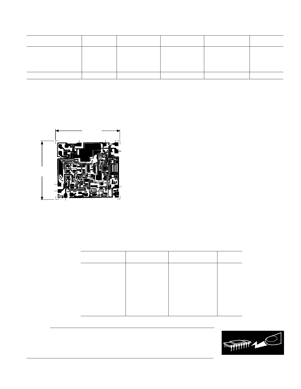
METALIZATION PHOTOGRAPH
Dimensions shown in inches and (mm).
0.074 (1.88)
NULL
+VS VOUT
8
7
6
7
8
6
5 OVER COMP
5
0.0677
(1.72)
NULL 1
–IN 2
1
2
3
3
+IN
4
4 –VS
ABSOLUTE MAXIMUM RATINGS1
Supply Voltage . . . . . . . . . . . . . . . . . . . . . . . . . . . . . . . . ± 18 V
Internal Power Dissipation2 . . . . . . . . . . . . . . . . . . . 650 mW
Input Voltage . . . . . . . . . . . . . . . . . . . . . . . . . . . . . . . . . . . ± VS
Differential Input Voltage3 . . . . . . . . . . . . . . . . . . . . . ± 0.7 V
Output Short Circuit Duration . . . . . . . . . . . . . . . . Indefinite
Storage Temperature Range (N, R) . . . . . . . –65°C to +125°C
Storage Temperature Range (Q) . . . . . . . . . –65°C to +150°C
Operating Temperature Range
AD705J/K . . . . . . . . . . . . . . . . . . . . . . . . . . . 0°C to +70°C
AD705A/B . . . . . . . . . . . . . . . . . . . . . . . . . –40°C to +85°C
AD705T . . . . . . . . . . . . . . . . . . . . . . . . . . –55°C to +125°C
Lead Temperature Range (Soldering 60 sec) . . . . . . . . +300°C
NOTES
1Stresses above those listed under “Absolute Maximum Ratings” may cause
permanent damage to the device. This is a stress rating only and functional
operation of the device at these or any other conditions above those indicated in
the operational section of this specification is not implied. Exposure to absolute
maximum rating conditions for extended periods may affect device reliability.
2Specification is for device in free air:
8-Pin Plastic Package:
θJA = 165°C/Watt
8-Pin Cerdip Package:
θJA = 110°C/Watt
8-Pin Small Outline Package: θJA = 155°C/Watt
3The input pins of these amplifiers are protected by back-to-back diodes. If the
differential voltage exceeds ± 0.7 V, external series protection resistors should be
added to limit the input current to less than 25 mA.
Model
AD705AQ
AD705BQ
AD705JCHIPS
AD705JN
AD705JR
AD705JR-REEL
AD705JR-REEL7
AD705KN
AD705TQ
AD705TQ/883B
ORDERING GUIDE
Temperature
Range
–40°C to +85°C
–40°C to +85°C
0°C to +70°C
0°C to +70°C
0°C to +70°C
0°C to +70°C
0°C to +70°C
0°C to +70°C
–55°C to +125°C
–55°C to +125°C
Package
Description
8-Pin Ceramic DIP
8-Pin Ceramic DIP
Bare Die
8-Pin Plastic DIP
8-Pin Plastic SOIC
8-Pin Plastic SOIC
8-Pin Plastic SOIC
8-Pin Plastic DIP
8-Pin Ceramic DIP
8-Pin Ceramic DIP
Package
Option
Q-8
Q-8
N-8
R-8
R-8
R-8
N-8
Q-8
Q-8
CAUTION
ESD (electrostatic discharge) sensitive device. Electrostatic charges as high as 4000 V readily
accumulate on the human body and test equipment and can discharge without detection.
Although the AD705 features proprietary ESD protection circuitry, permanent damage may
occur on devices subjected to high energy electrostatic discharges. Therefore, proper ESD
precautions are recommended to avoid performance degradation or loss of functionality.
WARNING!
ESD SENSITIVE DEVICE
REV. B
–3–
Share Link: 