MPSW56 Ver la hoja de datos (PDF) - ON Semiconductor
Número de pieza
componentes Descripción
Fabricante
MPSW56 Datasheet PDF : 4 Pages
| |||
ON Semiconductort
One Watt Amplifier Transistors
PNP Silicon
MAXIMUM RATINGS
Rating
Collector–Emitter Voltage
Collector–Base Voltage
Emitter–Base Voltage
Collector Current — Continuous
Total Device Dissipation @ TA = 25°C
Derate above 25°C
Total Device Dissipation @ TC = 25°C
Derate above 25°C
Operating and Storage Junction
Temperature Range
THERMAL CHARACTERISTICS
Characteristic
Thermal Resistance, Junction to Ambient
Thermal Resistance, Junction to Case
Symbol
VCEO
VCBO
VEBO
IC
PD
PD
TJ, Tstg
MPSW55 MPSW56
–60
–80
–60
–80
–4.0
–500
1.0
8.0
2.5
20
–55 to +150
Unit
Vdc
Vdc
Vdc
mAdc
Watt
mW/°C
Watts
mW/°C
°C
Symbol
RqJA
RqJC
Max
125
50
Unit
°C/W
°C/W
MPSW55
MPSW56*
*ON Semiconductor Preferred Device
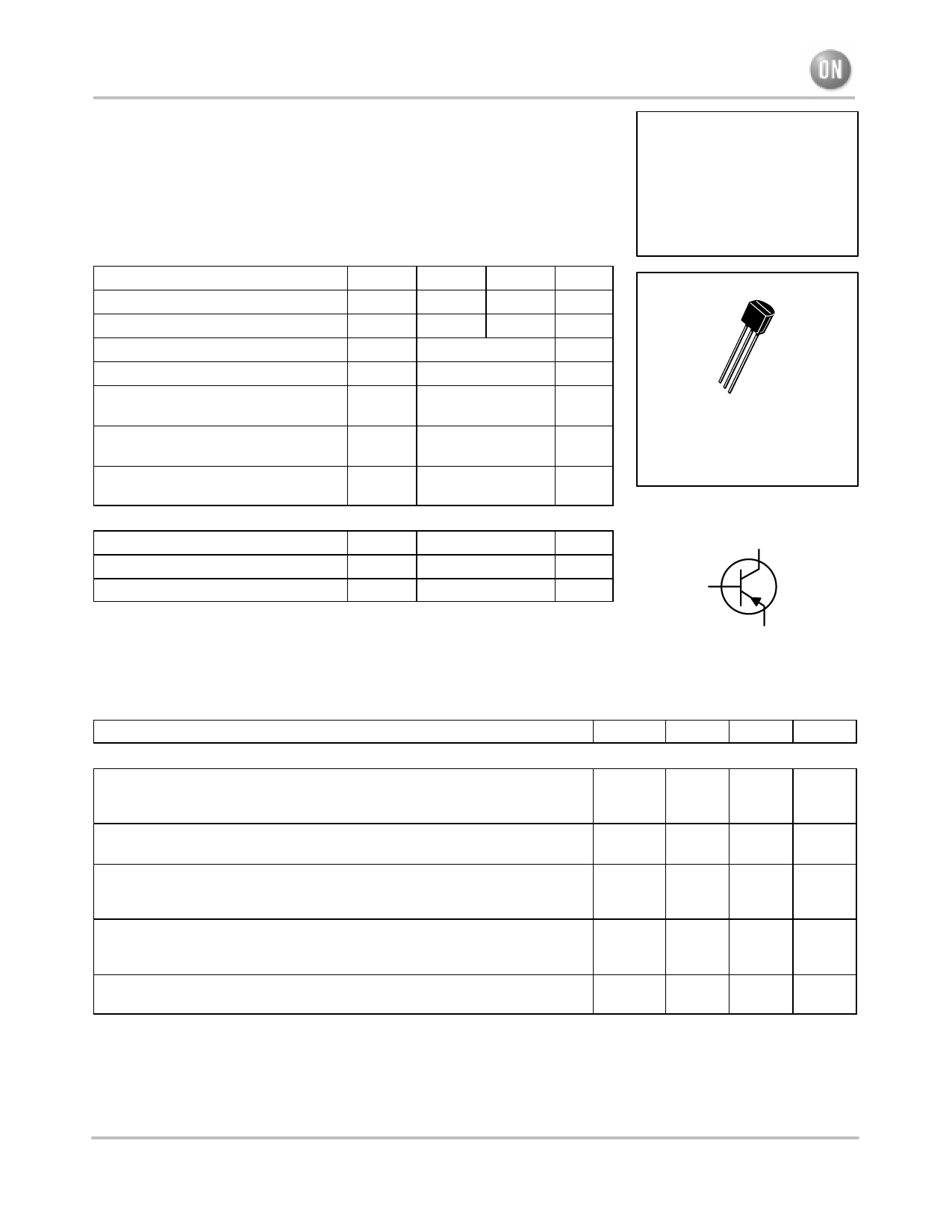
1
2
3
CASE 29–10, STYLE 1
TO–92 (TO–226AE)
COLLECTOR
3
2
BASE
1
EMITTER
ELECTRICAL CHARACTERISTICS (TA = 25°C unless otherwise noted)
Characteristic
OFF CHARACTERISTICS
Collector–Emitter Breakdown Voltage(1)
(IC = –1.0 mAdc, IB = 0)
MPSW55
MPSW56
Emitter–Base Breakdown Voltage
(IE = –100 mAdc, IC = 0)
Collector Cutoff Current
(VCE = –40 Vdc, IB = 0)
(VCE = –60 Vdc, IB = 0)
Collector Cutoff Current
(VCB = –40 Vdc, IE = 0)
(VCB = –60 Vdc, IE = 0)
Emitter Cutoff Current
(VEB = –3.0 Vdc, IC = 0)
MPSW55
MPSW56
MPSW55
MPSW56
1. Pulse Test: Pulse Width v 300 ms, Duty Cycle v 2.0%.
Symbol
Min
Max
Unit
V(BR)CEO
V(BR)EBO
ICES
ICBO
IEBO
–60
–80
–4.0
—
—
—
—
—
—
—
—
–0.5
–0.5
–0.1
–0.1
–0.1
Vdc
Vdc
µAdc
µAdc
µAdc
Preferred devices are ON Semiconductor recommended choices for future use and best overall value.
© Semiconductor Components Industries, LLC, 2001
1
March, 2001 – Rev. 1
Publication Order Number:
MPSW55/D
Share Link: 