TDA8740H Ver la hoja de datos (PDF) - Philips Electronics
Número de pieza
componentes Descripción
Fabricante
TDA8740H Datasheet PDF : 24 Pages
| |||
Philips Semiconductors
Satellite sound circuit with noise reduction
Product specification
TDA8740; TDA8740H
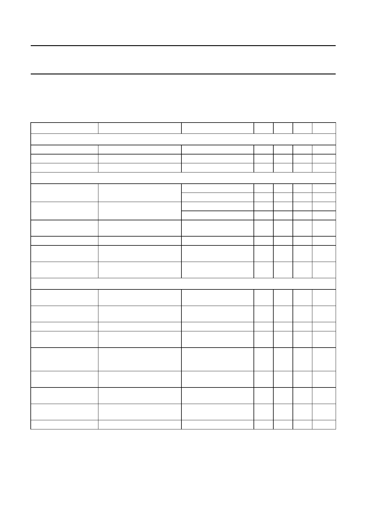
AC CHARACTERISTICS
All voltages referenced to ground at pins 9 and 34 (4 and 30). Measured in test circuit Fig.4; VP = 12 V; Tamb = 25 °C;
fMOD = 1 kHz; fOM = 6.5 MHz; ∆fM = 46 kHz; ∆fS1 = ∆fS2 = 27 kHz (reference levels); fOS1 = 7.02 MHz; fOS2 = 7.20 MHz;
HF level at pin 18 (14): 40 mV (RMS); HF level at selected secondary inputs: 20 mV (RMS); MCS = logic 0
[V7 (V2) = 0 V]; SCD = logic 0 [V11 (V6) = 0 V]; unless otherwise specified.
SYMBOL
PARAMETER
CONDITIONS
MIN. TYP. MAX. UNIT
Main channel - HF input pin 18 (14) and limiter
VIN3(rms)
VIN3(rms)
RIN3
input sensitivity (RMS value)
input signal level (RMS value)
input resistance
S/N(A) = 40 dB
Main channel - PLL FM demodulator and DC decoupling amplifier
fCCO
∆fOM
free-running frequency
lock range of PLL
MCS = logic 1
note 1
MCS = logic 1; note 1
RCDM
output resistance for 50 µs
de-emphasis pin 20 (16)
VCDM
∆VCDM
output voltage pin 20 (16)
spread of PLL output voltage
over lock range pin 20 (16)
RCCM
input resistance of output
amplifier pin 21 (17)
−
1.0 2.0 mV
−
−
200 mV
−
15 −
kΩ
−
6.5 −
MHz
−
10.7 −
MHz
5.5 −
7.5 MHz
10.0 −
11.5 MHz
1.24 1.5 1.7 kΩ
−18.5 −16.0 −14.5 dBV
−
−
±1 dB
95 150 200 kΩ
Main channel - overall performance (output selector in position 4)
VOM,OR,OL
output voltage pins 23, 24 and all PLLs locked
25 (19, 20 and 21)
−9 −6
UBM
output voltage unbalance pins output selector in
23, 24, 25 (19, 20, 21)
position 4
−0.5 −
THD
total harmonic distortion
all PLLs locked
−
0.1
S/N(A)
signal-to-noise ratio
A-weighted; all PLLs
locked
62 70
V--V---O-O---M-M---(--(1-1--5---k-k-H-H--z-z-)--)-
15 kHz frequency response
with respect to 1 kHz pin 23
(19)
no de-emphasis
connected
−0.5 0
ROM,OR,OL
output resistance pins 23, 24
and 25 (19, 20 and 21)
92 125
αS/M
crosstalk attenuation from
note 2
secondary channels to main
−
74
MUTEatt
mute attenuation
output selector in
position 7
74 −
SVRR
supply voltage ripple rejection VRR = 100 mV; fi = 70 Hz −
35
−4 dBV
+0.5 dB
0.5 %
−
dB
+0.5 dB
150 Ω
−
dB
−
dB
−
dB
October 1994
10
Share Link: 