LC74782 Ver la hoja de datos (PDF) - SANYO -> Panasonic
Número de pieza
componentes Descripción
Fabricante
LC74782 Datasheet PDF : 16 Pages
| |||
LC74782, 74782M
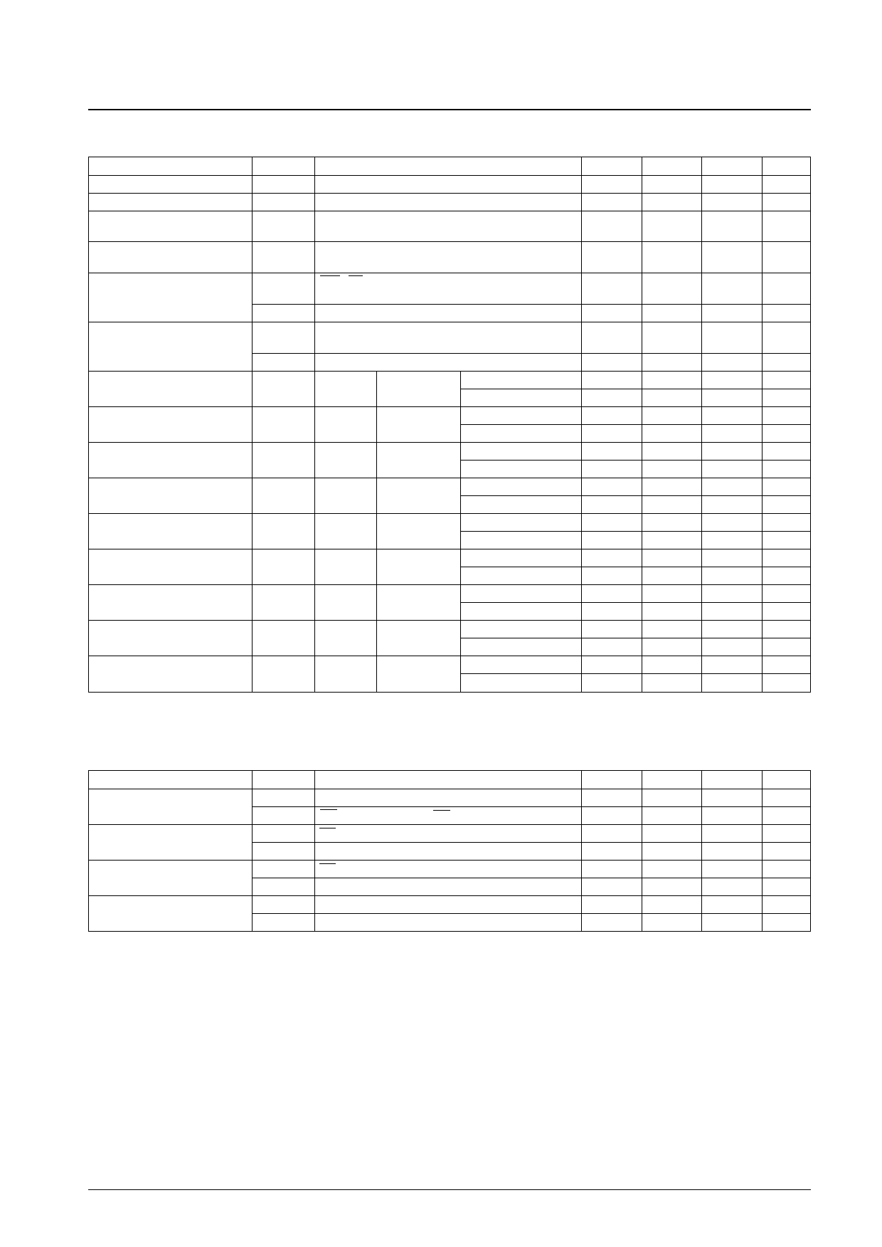
Electrical Characteristics at Ta = –30 to +70°C, VDD1 = 5 V unless otherwise specified
Parameter
Symbol
Conditions
min
Input off leakage current
Output off leakage current
Output high level voltage
Output low level voltage
Input current
Operating current drain
Sync level
Ileak1
Ileak2
VOH1
VOL1
IIH
IIL
IDD1
IDD2
VSN
CVIN pin
CVOUT pin
BLANK, CHARA and SEPOUT pins: VDD1 = 4.5 V,
IOH = –1.0 mA
BLANK, CHARA and SEPOUT pins: VDD1 = 4.5 V,
IOH = 1.0 mA
RST, CS, SIN, SCLK, CTRL1, CTRL3 and SEPIN pins:
VIN = VDD1
CTRL1, CTRL2, CTRL3 and OSCIN pins: VIN = VSS1
VDD1 pin; all outputs: open, Xtal: 7.159 MHz,
LC: 8 MHz
VDD2 pin: VDD2 = 5 V
CVOUT pin
VDD1 = 5.0 V,
VDD2 = 5.0 V
*1
*2
3.5
–1
0.70
0.91
Pedestal level
VPD
CVOUT pin
VDD1 = 5.0 V,
VDD2 = 5.0 V
*1
*2
1.31
1.53
Color burst low level
VCBL
CVOUT pin
VDD1 = 5.0 V,
VDD2 = 5.0 V
*1
*2
1.00
1.21
Color burst high level
VCBH
CVOUT pin
VDD1 = 5.0 V,
VDD2 = 5.0 V
*1
*2
1.63
1.84
Background color low level
VRSL
CVOUT pin
VDD1 = 5.0 V,
VDD2 = 5.0 V
*1
*2
1.47
1.68
Background color high level
VRSH
CVOUT pin
VDD1 = 5.0 V,
VDD2 = 5.0 V
*1
*2
1.99
2.19
Border level 0
VBK0
CVOUT pin
VDD1 = 5.0 V,
VDD2 = 5.0 V
*1
*2
1.42
1.63
Border level 1
VBK1
CVOUT pin
VDD1 = 5.0 V,
VDD2 = 5.0 V
*1
*2
1.99
2.19
Character level
VCHA
CVOUT pin
VDD1 = 5.0 V,
VDD2 = 5.0 V
*1
*2
2.58
2.78
Note: 1. When the sync level is 0.8 V.
2. When the sync level is 1.0 V.
typ
max
Unit
1
µA
1
µA
V
1.0
V
1
µA
µA
15
mA
20
mA
0.82
0.94
V
1.03
1.15
V
1.43
1.55
V
1.65
1.77
V
1.12
1.24
V
1.33
1.45
V
1.75
1.87
V
1.96
2.08
V
1.59
1.71
V
1.80
1.92
V
2.11
2.23
V
2.31
2.43
V
1.54
1.66
V
1.75
1.87
V
2.11
2.23
V
2.31
2.43
V
2.70
2.82
V
2.90
3.02
V
Timing Characteristics at Ta = –30 to +70°C, VDD1 = 5 ± 0.5 V
Parameter
Minimum input pulse width
Data setup time
Data hold time
One word write time
Symbol
tW (SCLK)
tW (CS)
tSU (CS)
tSU (SIN)
th (CS)
th (SIN)
tword
twt
Conditions
SCLK pin
CS pin (the period when CS is high)
CS pin
SIN pin
CS pin
SIN pin
8-bit data write time
RAM data write time
min
typ
max
Unit
200
ns
1
µs
200
ns
200
ns
2
µs
200
ns
4.2
µs
1
µs
No. 4989-4/16
Share Link: 