MT89L86 Ver la hoja de datos (PDF) - Mitel Networks
Número de pieza
componentes Descripción
Fabricante
MT89L86 Datasheet PDF : 40 Pages
| |||
MT89L86
Advance Information
Data Rate
2.048 Mb/s
4.096 Mb/s
8.192 Mb/s
Throughput Delay (d)
d=[32 + (32 - IN) + (OUT - 1)]; (expressed in # time-slots)
2.048 Mb/s time-slot: 3.9µs
IN: input time-slot (from 1 to 32)
OUT: output time-slot (from 1 to 32)
d=[64 + (64 - IN) + (OUT - 1)]; (expressed in # time-slots)
4.096 Mb/s time-slot: 1.95 µs
IN: input time-slot (from 1 to 64)
OUT: output time-slot (from 1 to 64)
d=[128 + (128 - IN) + (OUT - 1)]; (expressed in # time-slots)
8.192 Mb/s time-slot: 0.975 µs
IN: input time-slot (from 1 to 128)
OUT: output time-slot (from 1 to 128)
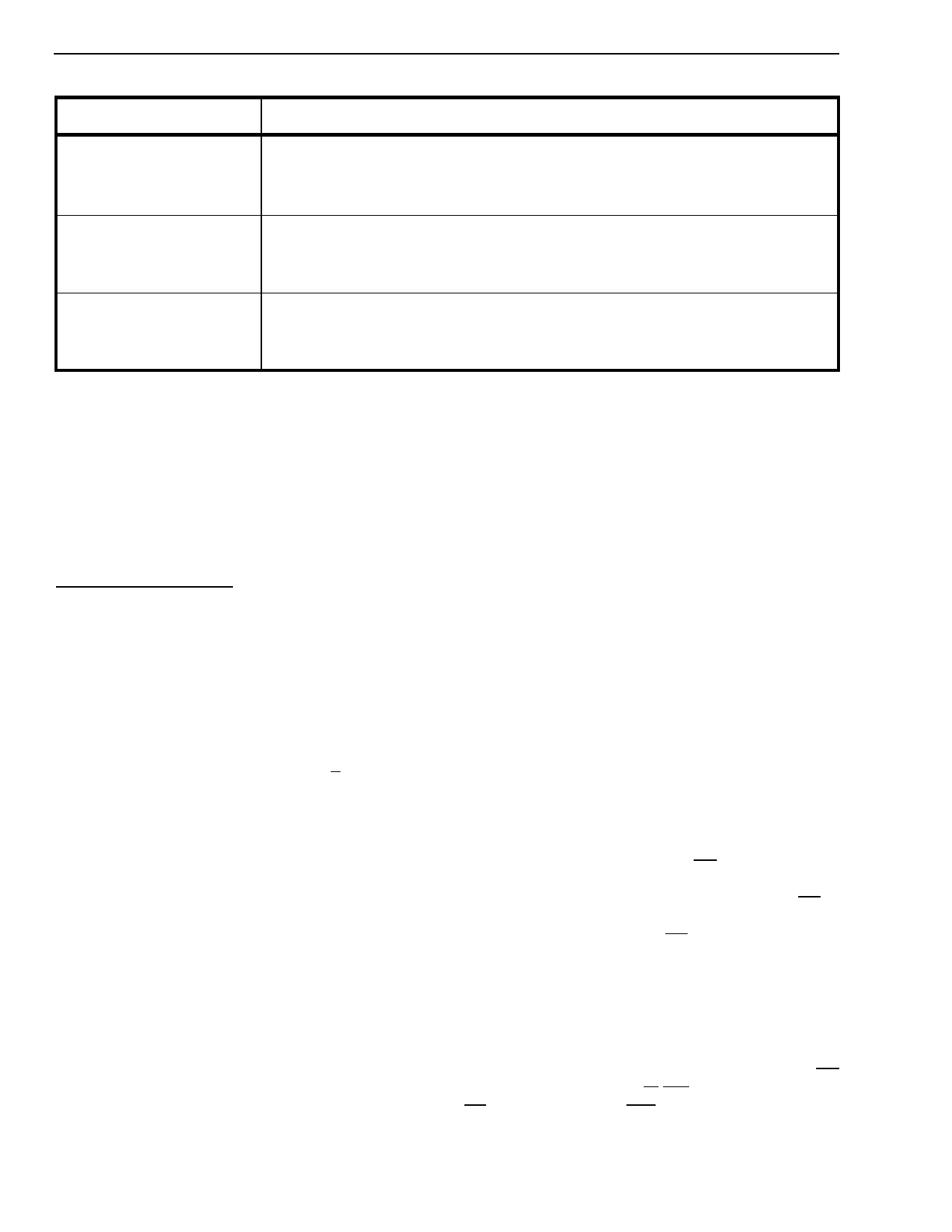
Table 4 - Constant Throughput Delay values
configurations with input and output channels that
provides more than its corresponding minimum
throughput delay, will have a throughput delay equal
to the difference between the output and input
channels; i.e., the throughput delay will be less than
one frame period. Table 3a shows the throughput
delay for each data rate operation.
Different I/O Data Rates
Except for the 2 Mb/s to 4 Mb/s and the 2 Mb/s to 8
Mb/s rate conversion operations, the throughput
delay from the MT89L86 may vary according to the
output stream used for switching.
Table 3b explains the worst case conditions for the
throughput delay when different I/O data rate
switching configurations are used.
Constant Throughput Delay mode (V/C bit = 1)
In this mode frame sequence integrity is maintained
in both Identical and Different I/O Data Rate
operations by making use of a multiple Data-Memory
buffer technique. The input channels written in any of
the buffers during frame N will be read out during
frame N+2. In applications at 2.048 Mb/s for
instance, the minimum throughput delay achievable
in constant delay mode will be 32 time-slots; for
example, when input time-slot 32 (channel 31) is
switched to output time-slot 1 (channel 0). Likewise,
the maximum delay is achieved when the first time
slot in a frame (channel 0) is switched to the last
time-slot in the frame (channel 31), resulting in 94
time-slots of delay.
To summarize, any input time-slot from input frame N
will always be switched to the destination time-slot
on output frame N+2. Table 4 describes the constant
throughput delay values at different data rates.
Microprocessor Port
The non-multiplexed bus interface provided by the
MT89L86 is identical to that provided in the MT8986
Digital Switch device. In addition to the non-
multiplexed bus, this 3.3V MT89L86 device provides
an enhanced microprocessor interface with
multiplexed bus structure compatible to both
Motorola and Intel buses. The multiplexed bus
structure is selected by the CPU Interface Mode (IM)
input pin.
If the IM input pin is connected to ground, the
MT89L86’s parallel port assumes its default Motorola
non-multiplexed bus mode identical to that of
MT8986. If the IM input is connected HIGH, the
internal parallel microprocessor port provides
compatibility to MOTEL (MOtorola and InTEL
compatible bus) interface allowing direct connection
to Intel, National and Motorola CPUs.
The on-chip MOTEL circuit automatically identifies
the type of CPU Bus connected to the device. This
circuit uses the level of the DS/RD input pin at the
rising edge of the AS/ALE to identify the appropriate
bus timing connected to the MT89L86. If DS/RD is
LOW at the rising edge of AS/ALE then the Motorola
bus timing is selected. If DS/RD is HIGH at the rising
edge of AS/ALE, the Intel bus timing is selected.
When the parallel port of this device is operating in
Motorola, National or Intel multiplexed bus
interfaces, the signals available for controlling the
device are: AD0-AD7 (Data and Address), ALE/AS
(Address Latch Enable/Address Strobe), DS/RD
(Data Strobe/Read), R/W\WR (Read/Write\Write),
CS (Chip Select) and DTA (Data Acknowledgment).
In the Motorola non-multiplexed bus mode, the
interface control signals are: data bus (AD0-AD7),
10
Share Link: 