UPC2710TB-E3 Ver la hoja de datos (PDF) - NEC => Renesas Technology
Número de pieza
componentes Descripción
Fabricante
UPC2710TB-E3 Datasheet PDF : 16 Pages
| |||
µPC2710TB
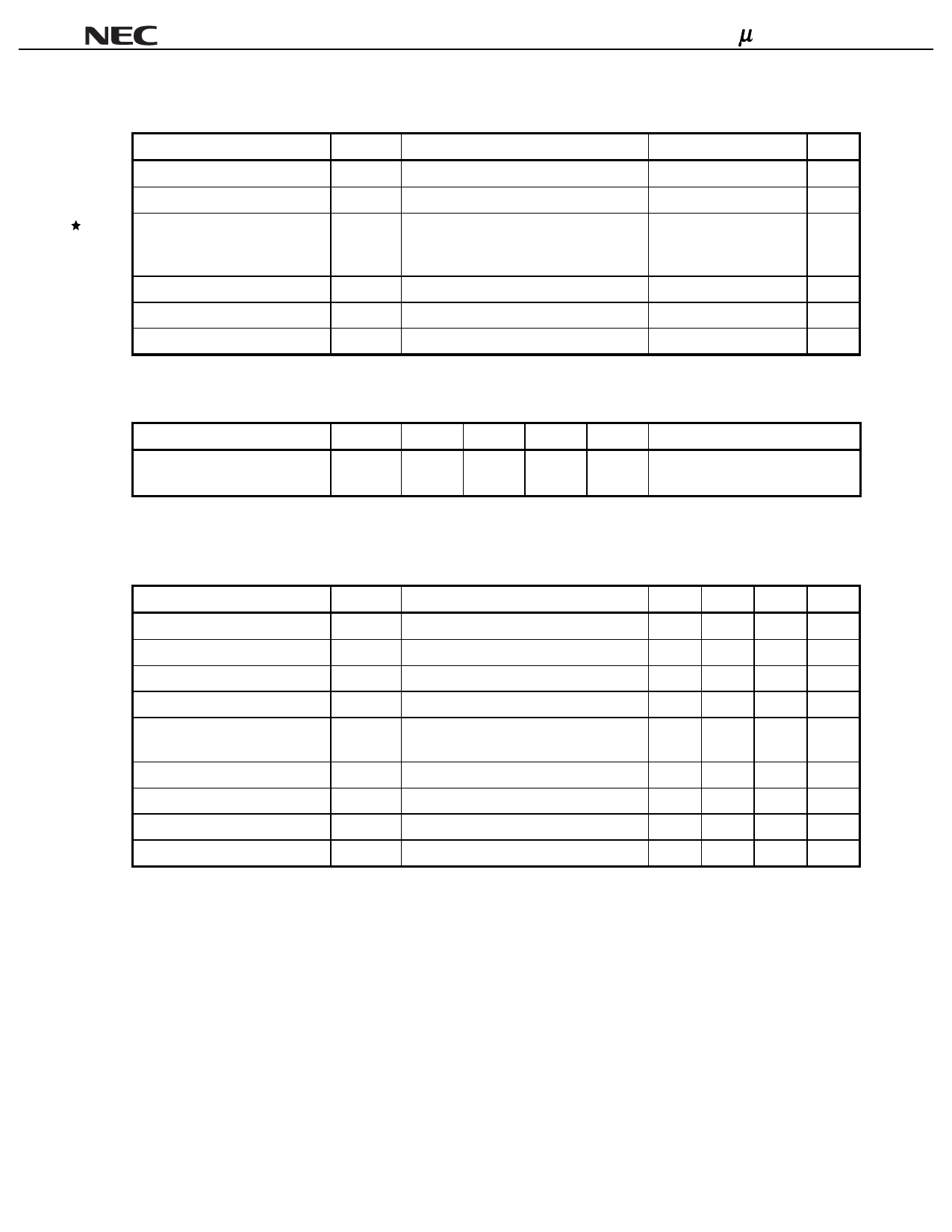
ABSOLUTE MAXIMUM RATINGS
Parameter
Supply Voltage
Total Circuit Current
Power Dissipation
Operating Ambient Temperature
Storage Temperature
Input Power
Symbol
VCC
ICC
PD
TA
Tstg
Pin
Conditions
TA = +25°C, pin 4 and pin 6
TA = +25°C
Mounted on double-sided copper clad
50 × 50 × 1.6 mm epoxy glass PWB
TA = +85°C
TA = +25°C
Ratings
5.8
60
270
−40 to +85
−55 to +150
+10
Unit
V
mA
mW
°C
°C
dBm
RECOMMENDED OPERATING RANGE
Parameter
Supply Voltage
Symbol
VCC
MIN.
4.5
TYP.
5.0
MAX.
5.5
Unit
Remark
V
The same voltage should be
applied to pin 4 and pin 6.
ELECTRICAL CHARACTERISTICS
(Unless otherwise specified, TA = +25°C, VCC = Vout = 5.0 V, ZS = ZL = 50 Ω)
Parameter
Circuit Current
Power Gain
Saturated Output Power
Noise Figure
Upper Limit Operating
Frequency
Isolation
Input Return Loss
Output Return Loss
Gain Flatness
Symbol
ICC
GP
PO(sat)
NF
fu
Test Conditions
No signal
f = 500 MHz
f = 500 MHz, Pin = –8 dBm
f = 500 MHz
3 dB down below flat gain at f = 0.1 GHz
MIN.
16
30
+11.0
–
0.7
TYP.
22
33
+13.5
3.5
1.0
MAX.
29
36.5
–
5.0
–
Unit
mA
dB
dBm
dB
GHz
ISL
RLin
RLout
∆GP
f = 500 MHz
f = 500 MHz
f = 500 MHz
f = 0.1 to 0.6 GHz
34
39
–
dB
3
6
–
dB
9
12
–
dB
–
±0.8
–
dB
Data Sheet P13443EJ3V0DS
5
Share Link: 