74LV14DB Ver la hoja de datos (PDF) - Nexperia B.V. All rights reserved
Número de pieza
componentes Descripción
Fabricante
74LV14DB Datasheet PDF : 18 Pages
| |||
Nexperia
74LV14
Hex inverting Schmitt trigger
11. Dynamic characteristics
Table 7. Dynamic characteristics
GND = 0 V; For test circuit see Figure 7.
Symbol Parameter
Conditions
Tamb = 40 C
to +85 C
Min Typ[1] Max
tpd
propagation delay nA to nY; see Figure 6
[2]
VCC = 1.2 V
-
80
-
VCC = 2.0 V
-
27
37
VCC = 2.7 V
-
VCC = 3.0 V to 3.6 V; CL = 15 pF [3] -
VCC = 3.0 V to 3.6 V
[3]
-
20
28
13
-
15
22
VCC = 4.5 V to 5.5 V
CPD
power dissipation CL = 50 pF; fi = 1 MHz;
capacitance
VI = GND to VCC
-
[4]
-
-
18
15
-
[1] All typical values are measured at Tamb = 25 C.
[2] tpd is the same as tPLH and tPHL.
[3] Typical values are measured at nominal supply voltage (VCC = 3.3 V).
[4] CPD is used to determine the dynamic power dissipation (PD in W).
PD = CPD VCC2 fi N + (CL VCC2 fo) where:
fi = input frequency in MHz, fo = output frequency in MHz
CL = output load capacitance in pF
VCC = supply voltage in V
N = number of inputs switching
(CL VCC2 fo) = sum of the outputs.
12. Waveforms
Tamb = 40 C
to +125 C
Min
Max
-
-
-
48
-
35
-
-
-
28
-
23
-
-
Unit
ns
ns
ns
ns
ns
ns
pF
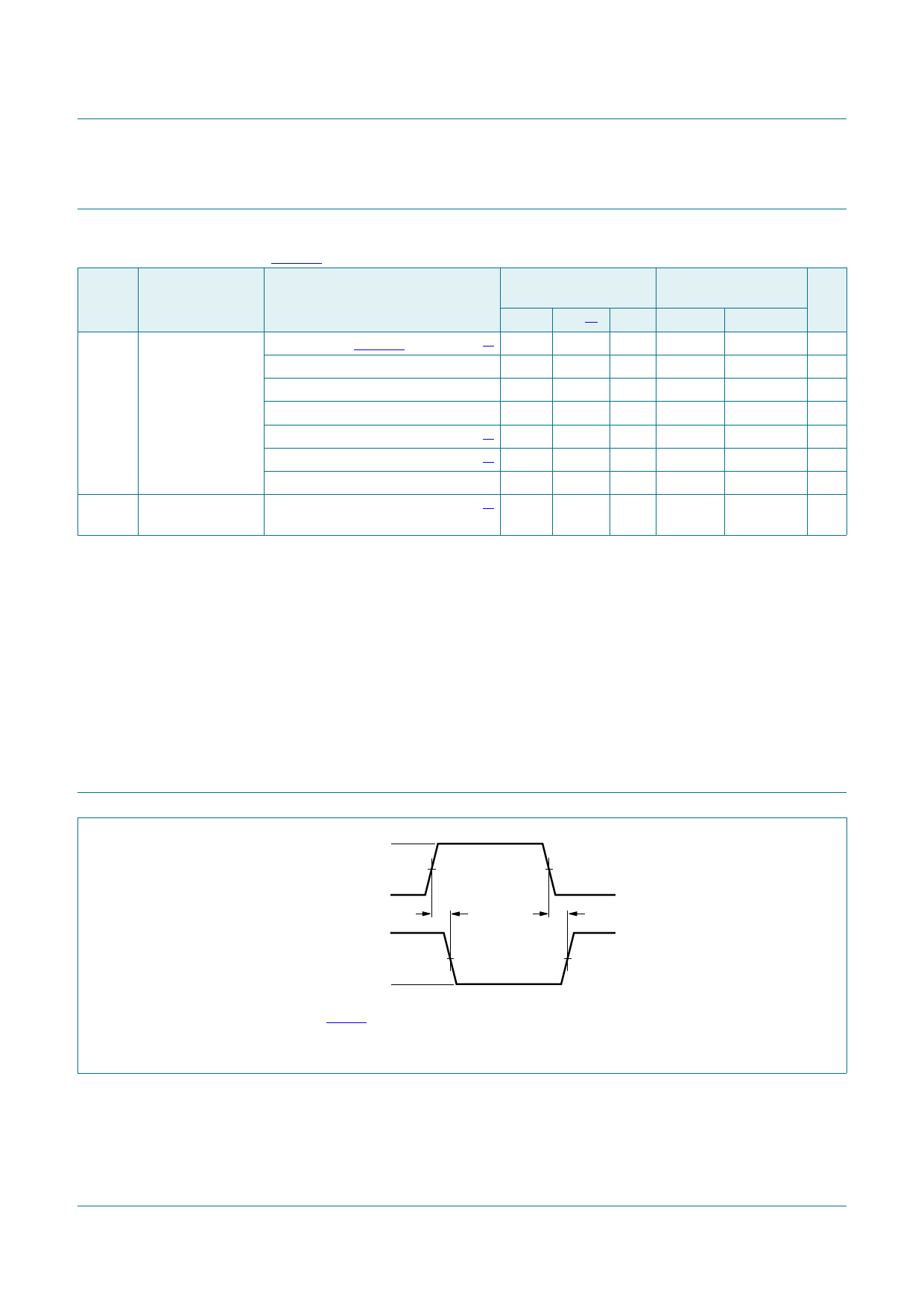
9,
Q$LQSXW
*1'
92+
Q<RXWSXW
92/
90
W 3+/
90
90
W3/+
90
PQD
Fig 6.
Measurement points are given in Table 8.
VOL and VOH are typical voltage output levels that occur with the output load.
The input (nA) to output (nY) propagation delays
74LV14
Product data sheet
All information provided in this document is subject to legal disclaimers.
Rev. 7 — 9 December 2015
© Nexperia B.V. 2017. All rights reserved
6 of 18
Share Link: 