M34D64-W Ver la hoja de datos (PDF) - STMicroelectronics
NГәmero de pieza
componentes DescripciГіn
Fabricante
M34D64-W
STMicroelectronics

M34D64-W Datasheet PDF : 27 Pages
| |||
M34D64-W
Device operation
3.5
Memory addressing
To start communication between the bus master and the slave device, the bus master must
initiate a Start condition. Following this, the bus master sends the Device Select Code,
shown in Table 2.: Device select code (on Serial Data (SDA), most significant bit first).
The Device Select Code consists of a 4-bit Device Type Identifier, and a 3-bit Chip Enable
вҖңAddressвҖқ (E2, E1, E0). To address the memory array, the 4-bit Device Type Identifier is
1010b.
Up to eight memory devices can be connected on a single I2C bus. Each one is given a
unique 3-bit code on the Chip Enable (E0, E1, E2) inputs. When the Device Select Code is
received on Serial Data (SDA), the device only responds if the Chip Enable Address is the
same as the value on the Chip Enable (E0, E1, E2) inputs.
The 8th bit is the Read/Write bit (RW). This bit is set to 1 for Read and 0 for Write operations.
If a match occurs on the Device Select code, the corresponding device gives an
acknowledgment on Serial Data (SDA) during the 9th bit time. If the device does not match
the Device Select code, it deselects itself from the bus, and goes into Standby mode.
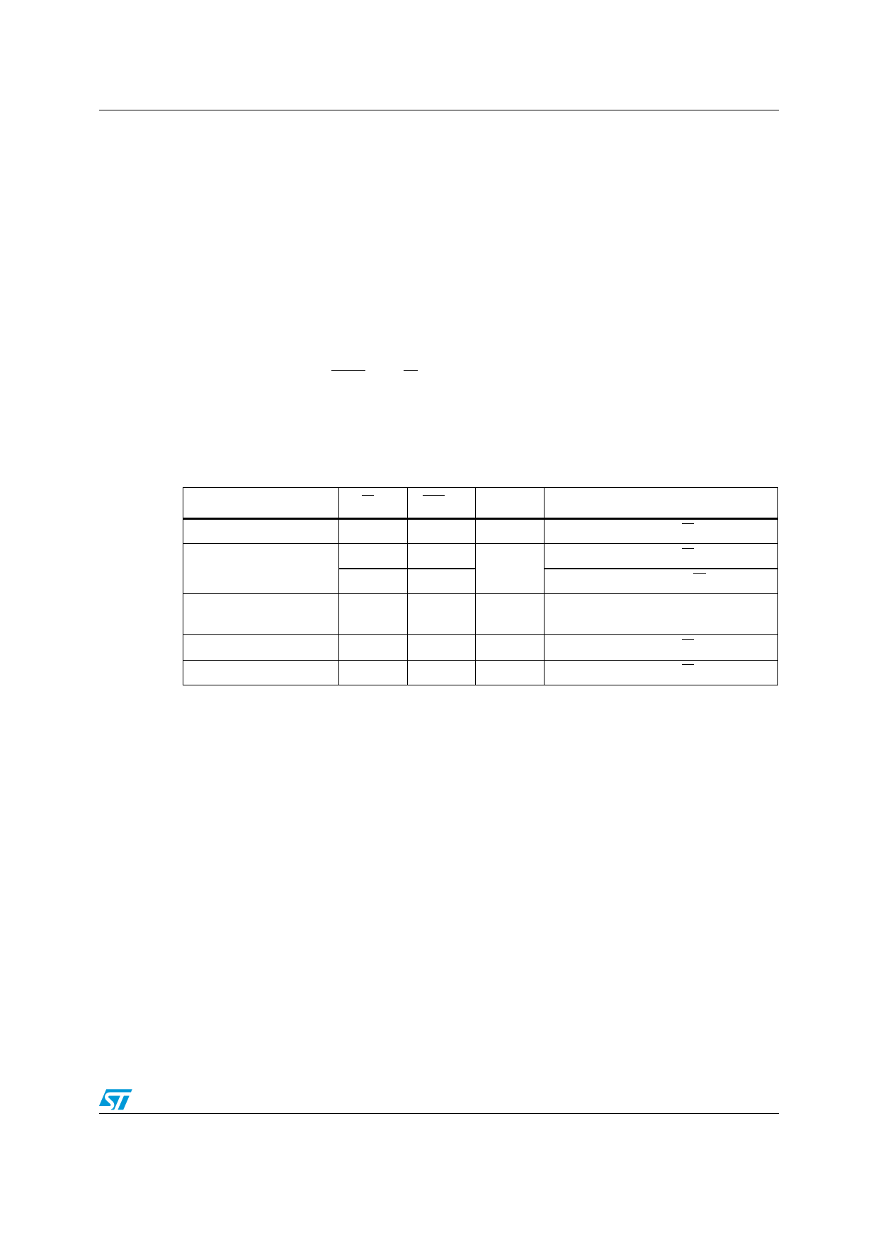
Table 5. Operating modes
Mode
RW bit
Current Address Read
1
0
Random Address Read
1
Sequential Read
1
Byte Write
0
Page Write
0
1. X = VIH or VIL.
WC (1)
X
X
X
X
VIL
VIL
Bytes
Initial sequence
1
Start, Device Select, RW = 1
Start, Device Select, RW = 0, Address
1
reStart, Device Select, RW = 1
вүҘ1
Similar to Current or Random Address
Read
1
Start, Device Select, RW = 0
вүӨ32 Start, Device Select, RW = 0
13/27
Share Link: