MGA-87563-BLKG Ver la hoja de datos (PDF) - Avago Technologies
Número de pieza
componentes Descripción
Fabricante
MGA-87563-BLKG Datasheet PDF : 9 Pages
| |||
It is recommended that the PCB traces for the ground pins
NOT be connected together underneath the body of the
package. PCB pads hidden under the package cannot be
adequately inspected for SMT solder quality.
FR-4 or G-10 PCB material is a good choice for most low
cost wireless applications. Typical board thickness is 0.025
or 0.031 inches. The width of 50 Ω microstriplines in these
PCB thicknesses is also convenient for mounting chip
components such as the series inductor at the input for
impedance matching or for DC blocking capacitors. For
noise figure sensitive applications, the use of PTFE/glass
dielectric materials may be warranted to minimize trans-
mission line losses at the amplifier input.
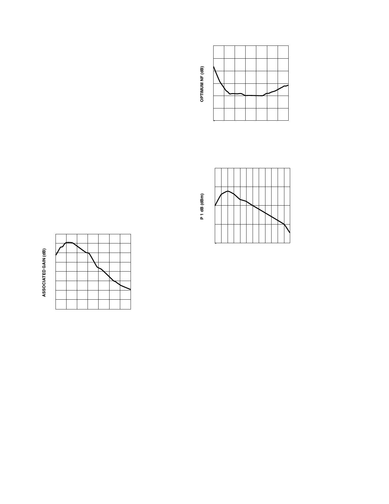
Higher Bias Voltages
While the MGA-87563 is designed for use in +3 volt bat-
tery powered applications, the internal bias regulation
circuitry allows it to be easily operated with any power
supply voltage from +2.7 to 5 volts. Figure 15 shows an
increase of approximately 1 dB in the associated gain with
+5 volts applied. The P1dB output power (Figure 17) is also
higher by about 1 dBm. The effect of higher Vdd on noise
figure is negligible as indicated in Figure 16.
17
16
15
14
13
12
11
10
9
0.5 1.0 1.5 2.0 2.5 3.0 3.5 4.0
FREQUENCY (GHz)
3.5
3.0
2.5
2.0
1.5
1.0
0.5
0.5 1.0 1.5 2.0 2.5 3.0 3.5 4.0
FREQUENCY (GHz)
Figure 16. Optimum Noise Figure vs. Frequency at Vdd = 5V.
0.00
-0.50
-1.00
-1.50
-2.00
0.6 1.2 1.8 2.4 3.0 3.6 4.2
FREQUENCY (GHz)
Figure 17. Output Power at 1 dB Gain Compression
vs. Frequency at Vdd = 5V.
Figure 15. Associated Gain vs. Frequency at Vdd = 5V.
7
Share Link: 