ISL59451 Ver la hoja de datos (PDF) - Renesas Electronics
Número de pieza
componentes Descripción
Fabricante
ISL59451 Datasheet PDF : 17 Pages
| |||
ISL59451
VIN
50
OR
75
ISL59451
x2
*CL
2.1pF
RL
150
VOUT
*CL Includes PCB trace capacitance
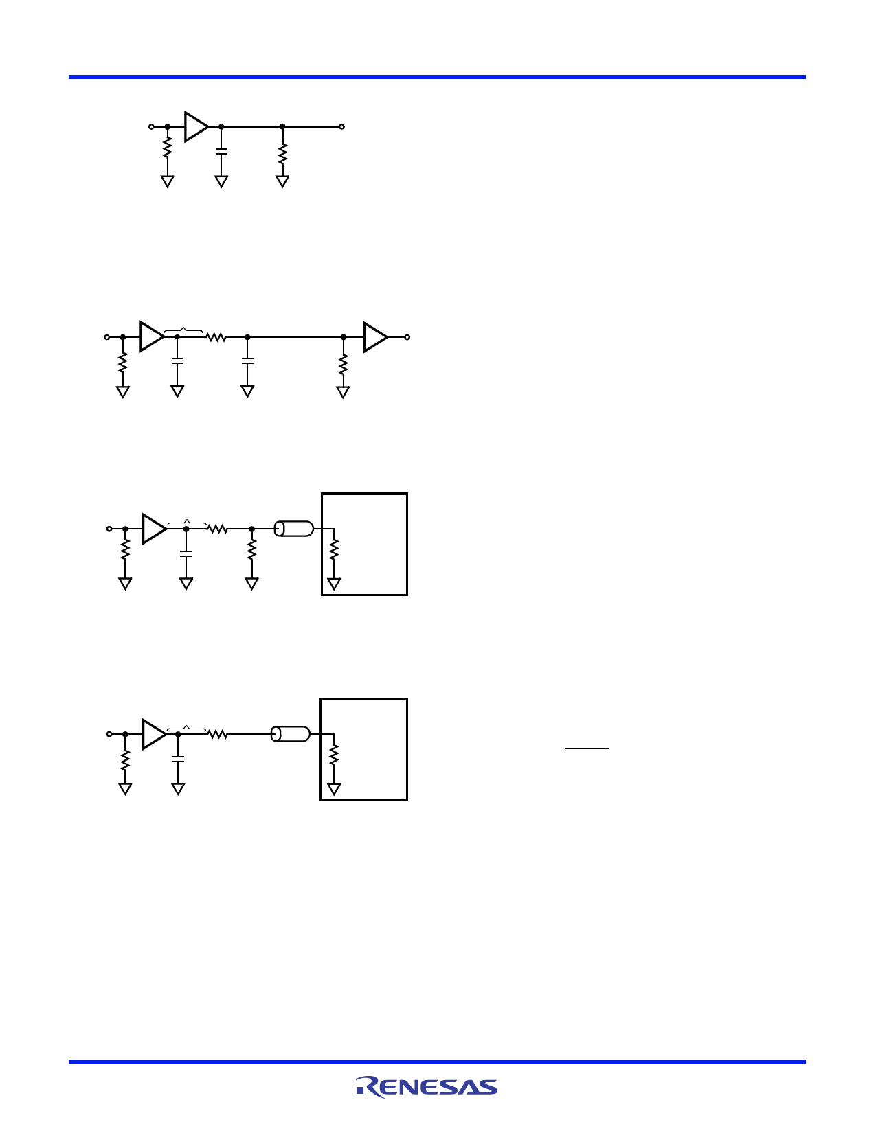
FIGURE 35A. TEST CIRCUIT WITH OPTIMAL OUTPUT LOAD
ISL59451 LCRIT
VIN
x2
50
OR
RS
CL
CS
75
RL
FIGURE 35B. INTER-STAGE APPLICATION CIRCUIT
VIN
50
ISL59451 LCRIT RS
x2
118
*CL
2.1pF
86.6
TEST
EQUIPMENT
50
*CL Includes PCB trace capacitance
FIGURE 35C. 150 TEST CIRCUIT WITH 50LOAD
ISL59451
VIN
LCRIT RS
x2
50
OR
50 or 75
*CL
75
2.1pF
TEST
EQUIPMENT
5075
*CL Includes PCB trace capacitance
FIGURE 35D. BACKLOADED TEST CIRCUIT FOR 5075
VIDEO CABLE APPLICATION
FIGURE 35. AC TEST CIRCUITS
AC Test Circuits
Figures 35A and 35B illustrate the optimum output load for
testing AC performance at 150 loads. Figure 35C illustrates
how to use the optimal 150load for a 50cable. Figure 35D
illustrates the optimum output load for 50 and 75 cable-
driving.
Application Information
General
The ISL59451 triple 4:1 MUX video driver features single +5V
supply operation, high bandwidth and TTL/CMOS logic
compatible gain select (AV2) of x1 (0dB) or x2 (+6dB). It also
includes a DC restore function to set the blanking level of the
output signal.
The ISL59451 implements the video DC-restore function with a
high performance gain-adjustable video amplifier and a nulling,
sample-hold amplifier to establish a user defined DC reference
voltage at the video amplifier output. A detailed description of
the DC-restore function implemented in the ISL59451 can be
found in application note AN1089, EL4089 and EL4390 DC-
Restored Video Amplifier. The ISL59451 performs the same
function with the exception that it is designed for single supply
operation. Each of the three output channels feature DC
restore functionality.
Video Amplifier Operation
(refer to “Functional Block Diagram” on page 12)
The ISL59451 video amplifier (A1) is a voltage-feed, high
performance video amplifier designed for +5V operation. The
output stage is capable of swinging to within 15mV of the
negative rail. The differential input stage contains an internal
voltage reference that positions the non-inverting input DC
level (V1) to ~1.6V higher than ground. This offset ensures that
the amplifier input DC level is maintained within the common
mode input voltage range. The amplifier non-inverting gain is
given in Equation 1.
VOUT
=
VI
N
+
–
1.6 V
1
+
R-R----G-F--
(EQ. 1)
DC-Restore Amplifier
(refer to “Functional Block Diagram” on page 12)
The DC-restore circuit contains a voltage reference amplifier
and an analog switch function that closes the DC-restore loop
under control of the CLAMP logic input. The A2 amplifier
output stage operates in a current-feedback mode with a
source capability of 860µA (Typ).
A logic “0” at the CLAMP input closes switch S1, which closes
the DC-restore loop. The video input AC coupling capacitor,
CX1, acts as a DC hold capacitor (through the 75termination
resistor) to average the current-source output of amplifier A2.
When the DC-restore loop has reached equilibrium, the DC
voltage stored on CX1 will be the value required to set the
voltages at A1 (VOUT) and A2 (VIN+) according to Equations 2
and 3:
VOUT(DC) = VREF
(EQ. 2)
VIN+ = VOUT(DC) + 1.6V
(EQ. 3)
FN6253 Rev 0.00
September 24, 2007
Page 14 of 17
Share Link: 