M95010 Ver la hoja de datos (PDF) - STMicroelectronics
Número de pieza
componentes Descripción
Fabricante
M95010 Datasheet PDF : 32 Pages
| |||
M95040, M95020, M95010
SIGNAL DESCRIPTION
VCC must be held within the specified range:
VCC(min) to VCC(max).
All of the input and output signals can be held High
or Low (according to voltages of VIH, VOH, VIL or
VOL, as specified in Tables 12 to 16). These sig-
nals are described next.
Serial Data Output (Q)
This output signal is used to transfer data serially
out of the device. Data bytes are shifted out on the
falling edge of the Serial Clock (C).
Serial Data Input (D)
This input signal is used to transfer data serially
into the device. Instructions, addresses, and input
data bytes are shifted in on the rising edge of the
Serial Clock (C).
Serial Clock (C)
This input signal provides the timing for the serial
interface.
Chip Select (S)
When this input signal is High, the device is dese-
lected, and the Serial Data Output (Q) is high im-
pedance.
Hold (HOLD)
This input signal is used to pause temporarily any
serial communications with the device, without los-
ing bits that have already been passed on the se-
rial bus.
Write Protect (W)
This input signal is used to control whether the
memory is write protected. When W is held Low,
writes to the memory are disabled, but other oper-
ations remain enabled. No action on this signal, or
on the Write Enable Latch (WEL) bit, can interrupt
a Write cycle that has already started.
CONNECTING TO THE SPI BUS
These devices are fully compatible with the SPI
protocol.
All instructions, addresses and input data bytes
are shifted in to the device, most significant bit
first. The Serial Data Input (D) is sampled on the
first rising edge of the Serial Clock (C) after Chip
Select (S) goes Low.
All output data bytes are shifted out of the device,
most significant bit first. The Serial Data Output
(Q) is latched on the first falling edge of the Serial
Clock (C) after the instruction (such as the Read
from Memory Array and Read Status Register
instructions) have been clocked into the device.
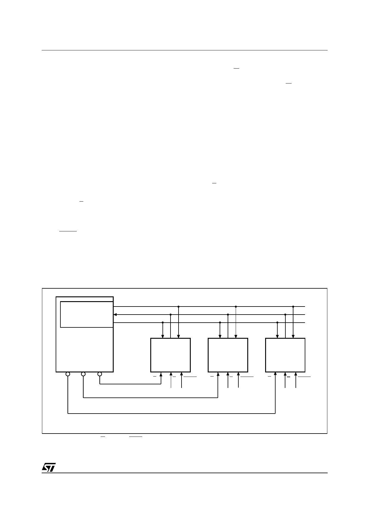
Figure 5 shows three devices, connected to an
MCU, on a SPI bus. Only one device is selected at
a time, so only one device drives the Serial Data
Output (Q) line at a time, all the others being high
impedance.
Figure 5. Bus Master and Memory Devices on the SPI Bus
SPI Interface with
(CPOL, CPHA) =
(0, 0) or (1, 1)
Bus Master
(ST6, ST7, ST9,
ST10, Others)
SDO
SDI
SCK
CS3 CS2 CS1
CQD
CQD
CQD
SPI Memory
Device
SPI Memory
Device
SPI Memory
Device
S
W HOLD
S
W HOLD
S
W HOLD
Note: 1. The Write Protect (W) and Hold (HOLD) signals should be driven, High or Low as appropriate.
AI03746D
3/32
Share Link: 