LB1823 Ver la hoja de datos (PDF) - SANYO -> Panasonic
Número de pieza
componentes Descripción
Fabricante
LB1823 Datasheet PDF : 11 Pages
| |||
LB1823
• Output transistors
The output transistors must be chosen according to the current and breakdown voltage settings determined by the
required motor power. Printed circuit board space considerations determine the choice of discrete or driver array
components.
Upper side transistors
(Darlington)
2SA1259
2SB881
2SB882
2SB883
Lower side transistors
2SD1060
2SD1061
2SD1062
2SD1065
Current
5A
7A
10 A
15 A
Breakdown voltage
50 V
50 V
50 V
50 V
The 2SC4070 (SPA) and 2SC4113 (SPA) lower side predriver transistors include an emitter-base resistor.
When no resistor is required, the same transistors as used in the output interface can be used.
Driver arrays:
SLA6022 and SLA6023 (Sanken)
12. Through currents due to the direct PWM technique
In the direct PWM technique through currents flow in the outputs due to the switching, e.g., when used in a discrete
structure (including predriver circuits) or in LB1822 applications. These through currents are due to the delays and
parasitic capacitances in the output transistors. Although additional capacitors were previously used to deal with this
problem, the LB1823 includes circuit modifications to ameliorate through currents. However, even despite these
measures, through currents can still occur if the values of R17, R18 and R19 are made too large, since the switching
time of the lower side transistors will be increased. Although whiskers of under 10 ns can be seen in the Rf voltage
waveform during switching, this will not be a problem. (These occur in the probe and do not correspond to current
flows.)
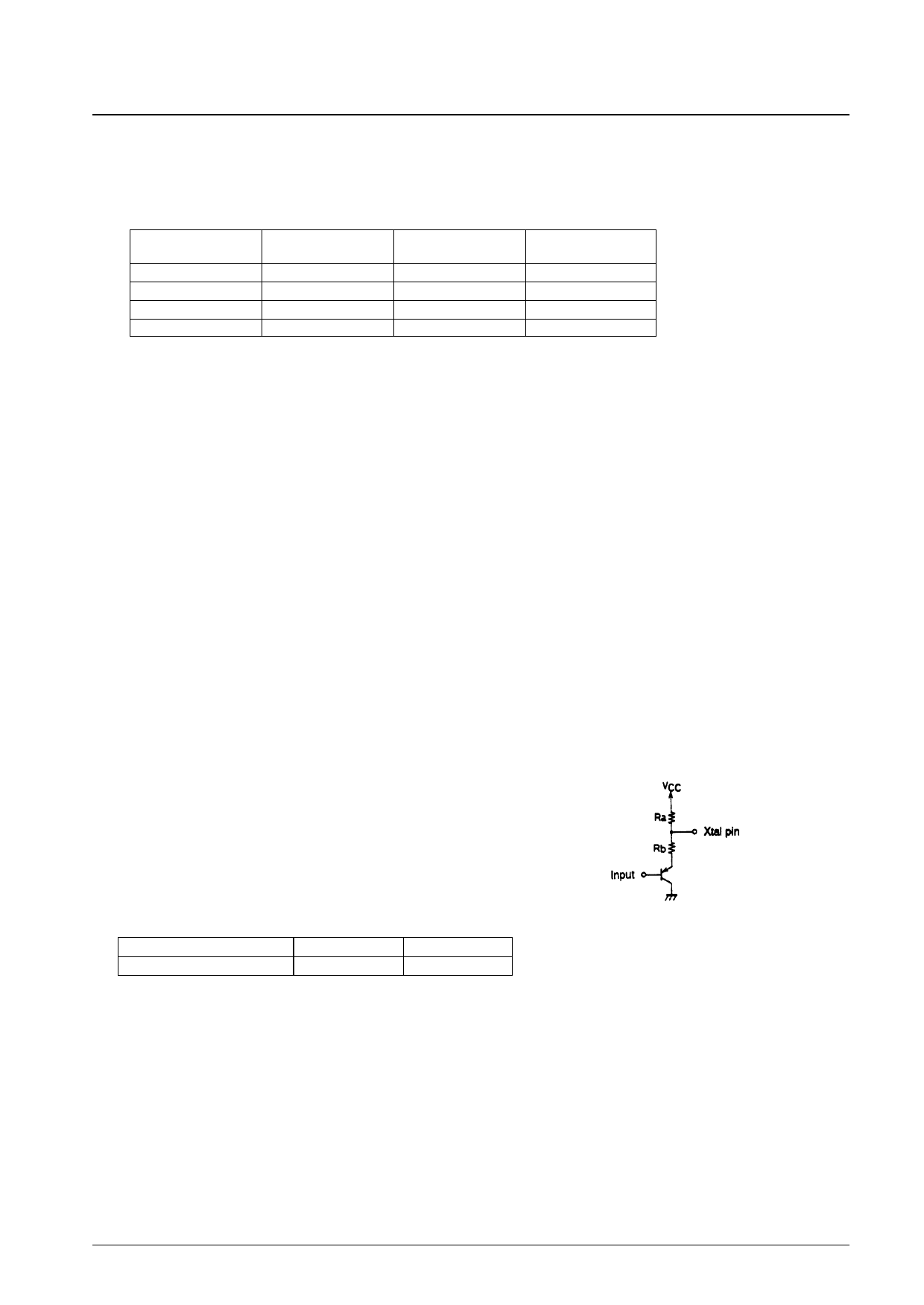
13. Oscillator element
Normally, a crystal resonator, a resistors, and two capacitors are connected to the LB1823 Xtal pin. A ceramic
oscillator could also be used in applications that do not require such precise speed control characteristics. To avoid
problems, consult with the manufacturer of the oscillator element when selecting the oscillator element and the
values of the external resistor and capacitors used. Use a circuit consisting of resistors and a pnp transistor as shown
in the figure to apply an external clock signal (CLK) to the Xtal pin.
fCLK = 1 to 10.2 MHz
Input signal levels
High level voltage: 4.0 V minimum
Low level voltage: 1.5 V maximum
Capacitors must be added to this circuit if overshoot
and/or undershoot appears in the input waveform. Be
sure to check for this condition in that case.
Reference values
VCC = 6.3 V typ (5.8 to 6.8 V)
VCC = 5.0 V typ (4.5 to 5.5 V)
Ra = 1.5 kΩ
Ra = 2.0 kΩ
Rb = 2.0 kΩ
Rb = 1.0 kΩ
No. 4263-10/11
Share Link: 