M29W320DB70N1E_03 Ver la hoja de datos (PDF) - STMicroelectronics
Número de pieza
componentes Descripción
Fabricante
M29W320DB70N1E_03 Datasheet PDF : 44 Pages
| |||
M29W320DT, M29W320DB
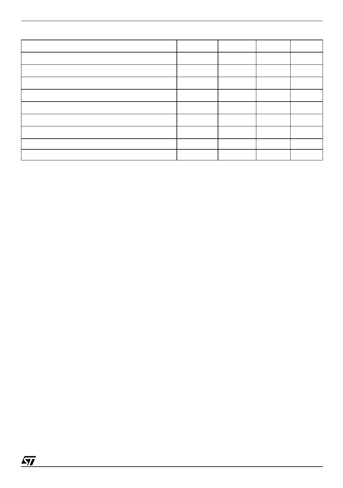
Table 6. Program, Erase Times and Program, Erase Endurance Cycles
Parameter
Min
Typ (1, 2)
Max(2)
Unit
Chip Erase
40
200(3)
s
Block Erase (64 KBytes)
0.8
6(4)
s
Erase Suspend Latency Time
15
25(4)
µs
Program (Byte or Word)
10
200(3)
µs
Accelerated Program (Byte or Word)
8
150(3)
µs
Chip Program (Byte by Byte)
40
200(3)
s
Chip Program (Word by Word)
20
100(3)
s
Program/Erase Cycles (per Block)
100,000
cycles
Data Retention
20
years
Note: 1. Typical values measured at room temperature and nominal voltages.
2. Sampled, but not 100% tested.
3. Maximum value measured at worst case conditions for both temperature and VCC after 100,00 program/erase cycles.
4. Maximum value measured at worst case conditions for both temperature and VCC.
STATUS REGISTER
Bus Read operations from any address always
read the Status Register during Program and
Erase operations. It is also read during Erase Sus-
pend when an address within a block being erased
is accessed.
The bits in the Status Register are summarized in
Table 7, Status Register Bits.
Data Polling Bit (DQ7). The Data Polling Bit can
be used to identify whether the Program/Erase
Controller has successfully completed its opera-
tion or if it has responded to an Erase Suspend.
The Data Polling Bit is output on DQ7 when the
Status Register is read.
During Program operations the Data Polling Bit
outputs the complement of the bit being pro-
grammed to DQ7. After successful completion of
the Program operation the memory returns to
Read mode and Bus Read operations from the ad-
dress just programmed output DQ7, not its com-
plement.
During Erase operations the Data Polling Bit out-
puts ’0’, the complement of the erased state of
DQ7. After successful completion of the Erase op-
eration the memory returns to Read Mode.
In Erase Suspend mode the Data Polling Bit will
output a ’1’ during a Bus Read operation within a
block being erased. The Data Polling Bit will
change from a ’0’ to a ’1’ when the Program/Erase
Controller has suspended the Erase operation.
Figure 7, Data Polling Flowchart, gives an exam-
ple of how to use the Data Polling Bit. A Valid Ad-
dress is the address being programmed or an
address within the block being erased.
Toggle Bit (DQ6). The Toggle Bit can be used to
identify whether the Program/Erase Controller has
successfully completed its operation or if it has re-
sponded to an Erase Suspend. The Toggle Bit is
output on DQ6 when the Status Register is read.
During Program and Erase operations the Toggle
Bit changes from ’0’ to ’1’ to ’0’, etc., with succes-
sive Bus Read operations at any address. After
successful completion of the operation the memo-
ry returns to Read mode.
During Erase Suspend mode the Toggle Bit will
output when addressing a cell within a block being
erased. The Toggle Bit will stop toggling when the
Program/Erase Controller has suspended the
Erase operation.
If any attempt is made to erase a protected block,
the operation is aborted, no error is signalled and
DQ6 toggles for approximately 100µs. If any at-
tempt is made to program a protected block or a
suspended block, the operation is aborted, no er-
ror is signalled and DQ6 toggles for approximately
1µs.
Figure 8, Data Toggle Flowchart, gives an exam-
ple of how to use the Data Toggle Bit.
Error Bit (DQ5). The Error Bit can be used to
identify errors detected by the Program/Erase
Controller. The Error Bit is set to ’1’ when a Pro-
gram, Block Erase or Chip Erase operation fails to
write the correct data to the memory. If the Error
Bit is set a Read/Reset command must be issued
19/44
Share Link: 