UAA3522HL Ver la hoja de datos (PDF) - Philips Electronics
Número de pieza
componentes Descripción
Fabricante
UAA3522HL Datasheet PDF : 28 Pages
| |||
Philips Semiconductors
Low power dual-band GSM transceiver
with an image rejecting front-end
Objective specification
UAA3522HL
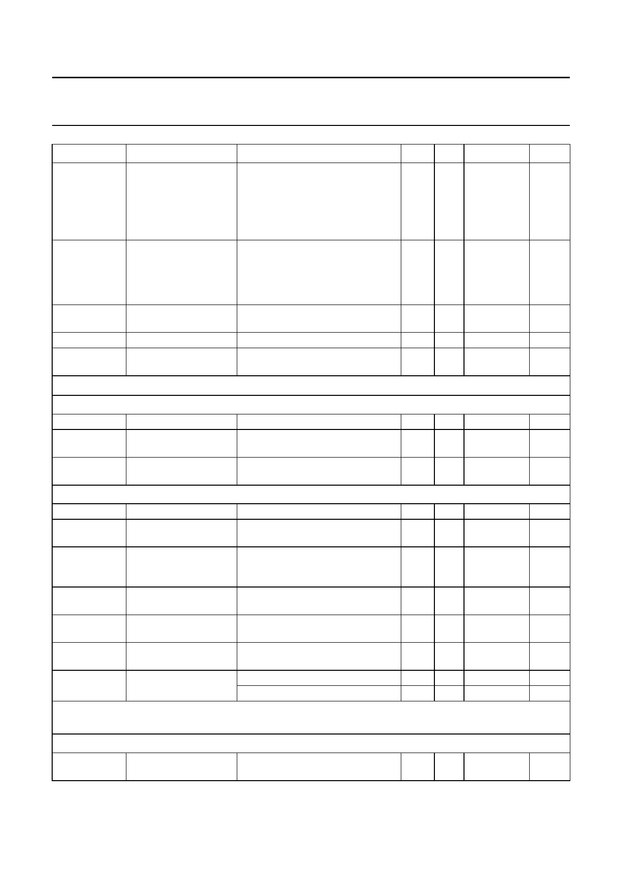
SYMBOL
PARAMETER
CONDITIONS
MIN. TYP. MAX.
αbf5
baseband filter
note 10;
attenuation
(fifth-order Butterworth)
∆fmod = 140 kHz
∆fmod = 200 kHz
∆fmod = 400 kHz
8
11 −
19 25 −
36 55 −
∆fmod = 600 kHz
44 − −
Vo(pin)(peak)(max) maximum peak output differential resistance between
0.75 − −
voltage per pin giving a QA/QB or IA/IB > = 180 kΩ; note 1
total harmonic
distortion of less
than 3% at Gconv >7
VOO
output offset voltage Gconv = 31 dB
adjustment
−60 − +60
LSBoffset
∆Voffset
LSB offset adjustment
offset variation
gain from Gconv(dif)(min)
to Gconv(dif)(max)
−
50 100
−10 − +10
Transmit IF section; general conditions: Vmod(peak) = 0.25 V; VI(IQ) = VO(IQ) = 1.25 V; fmod = 67.7 kHz
BASEBAND INPUT/OUT; TX MODE (PINS IA, IB, QA AND QB)
∆fmod
Vmod(peak)
DRi
modulation frequency
modulation level (peak
value)
dynamic input
resistance
gain = −3 dB gain
single-ended
single-ended per pin
0
−2
0.225 0.25 0.275
−
12.5 −
TRANSMITTER IF LC TUNED CIRCUIT (PINS TXIFA AND TXIFB)
fo(IF)
LOout
IF output frequency
local oscillator
feedthrough level
fo(IF) = 200 MHz
−
200 −
−
−40 −30
Po
transmit power without fo(IF) = 200 MHz
−
−16 −
LC tuned circuit
± 67.7 kHz; measured through a
balun; note 12
IM2o
level of second-order
image products
fo(IF) = 200 MHz
± 2 × 67.7 kHz; note 12
−
−48 −45
IM3o
level of third-order
image products
fo(IF) = 200 MHz
± 3 × 67.7 kHz; note 12
−
−55 −50
IMo
image level
fo(IF) = 200 MHz
− 67.7 kHz; note 12
−
−34 −
ϕN
phase noise output
foffset = 400 kHz
power density
foffset = 10 MHz
−
− −125
−
−140 −133
Transmit modulation loop section; General conditions: Vmod(peak) = 0.25 V; VI(IQ) = VO(IQ) = 1.25 V;
fmod = 67.7 kHz
OFFSET MIXER; GSM BAND (PINS TXIRFA AND TXIRFB)
fi(RF)(TX)
TX RF VCO input
frequency
880 − 915
UNIT
dB
dB
dB
dB
V
mV
mV
mV
MHz
V
kΩ
MHz
dBc
dBm
dBc
dBc
dBc
dBc/Hz
dBc/Hz
MHz
2000 Feb 18
15
Share Link: 