MC33349N-7 Ver la hoja de datos (PDF) - Motorola => Freescale
Número de pieza
componentes Descripción
Fabricante
MC33349N-7 Datasheet PDF : 8 Pages
| |||
MC33349
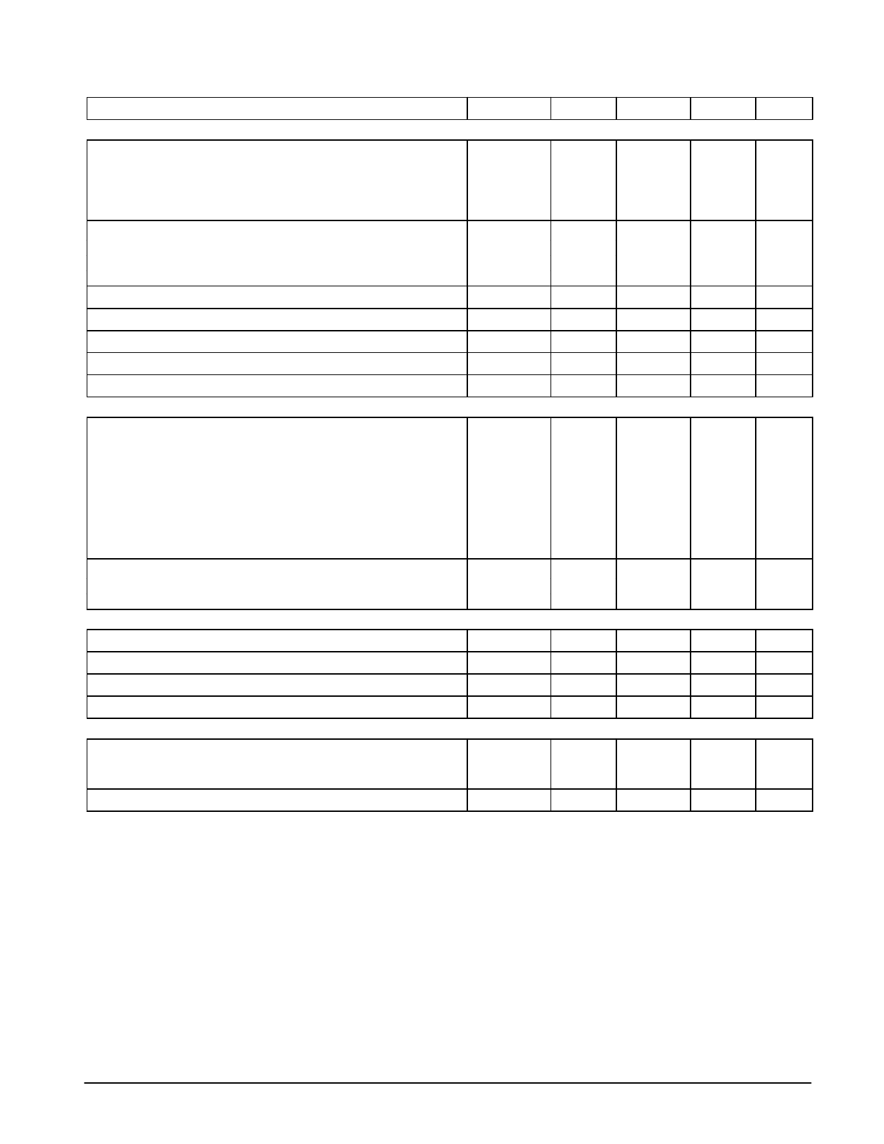
ELECTRICAL CHARACTERISTICS (Ct = 0.01 µF, TA = 25°C, for min/max values TA is the operating junction temperature range
that applies, unless otherwise noted.)
Characteristic
Symbol
Min
Typ
Max
Unit
ÁÁÁÁÁÁÁÁÁÁÁÁÁÁÁÁÁÁÁÁÁÁÁÁÁÁÁÁÁÁÁÁÁÁÁÁÁÁÁÁÁÁÁÁÁÁÁÁÁÁÁÁÁÁÁÁÁÁÁÁÁÁÁÁÁÁÁÁ VOLTAGE SENSING
Cell Charging Cutoff (Pin 5 to Pin 6)
Overvoltage Threshold, VCell Increasing
Vth(OV)
V
–1, –3 Suffix
–
4.35
–
ÁÁÁÁÁÁÁÁÁÁÁÁÁÁÁÁÁÁÁÁÁÁÁÁÁÁÁÁÁÁÁÁÁÁÁÁÁÁÁÁÁÁÁÁÁÁÁÁÁÁÁÁÁÁÁÁÁÁÁÁÁÁÁÁÁÁÁÁ –2, –4 Suffix
Overvoltage Hysteresis VCell Decreasing
Cell Discharging Cutoff (Pin 5 to Pin 6)
–
4.25
–
VH
–
200
–
mV
Undervoltage Threshold, VCell Decreasing
Vth(UV)
V
–1, –3 Suffix
–2, –4 Suffix
ÁÁÁÁÁÁÁÁÁÁÁÁÁÁÁÁÁÁÁÁÁÁÁÁÁÁÁÁÁÁÁÁÁÁÁÁÁÁÁÁÁÁÁÁÁÁÁÁÁÁÁÁÁÁÁÁÁÁÁÁÁÁÁÁÁÁÁÁ Input Bias Current During Cell Voltage Sample (Pin 5)
–
2.30
–
–
2.28
–
IIIB
–
20
–
µA
Overvoltage Delay Time (Vcell = 4.5 V)
Unervoltage Delay Time (Vcell = 2.1 V)
ÁÁÁÁÁÁÁÁÁÁÁÁÁÁÁÁÁÁÁÁÁÁÁÁÁÁÁÁÁÁÁÁÁÁ Cell Voltage Sampling Period
ÁÁÁÁÁÁÁÁÁÁÁÁÁÁÁÁÁÁÁÁÁÁÁÁÁÁÁÁÁÁÁÁÁÁ Cell Voltage Sampling Repitition Period
ÁÁÁÁÁÁÁÁÁÁÁÁÁÁÁÁÁÁÁÁÁÁÁÁÁÁÁÁÁÁÁÁÁÁ CURRENT SENSING
ÁÁÁÁÁÁÁÁÁÁÁÁÁÁÁÁÁÁÁÁÁÁÁÁÁÁÁÁÁÁÁÁÁÁ Discharge/Charge Current Limit (Pin 2 to Pin 6)
ÁÁÁÁÁÁÁÁÁÁÁÁÁÁÁÁÁÁÁÁÁÁÁÁÁÁÁÁÁÁÁÁÁÁ Discharge Threshold Voltage
t(ovd)
–
75
–
ms
t(uvd)
–
13
–
ms
t(smpl)
–
2.0
–
ms
t(rep)
–
26
–
ms
Vth(dschg)
mV
–1, –2 Suffix
–
150
–
–3, –4 Suffix
–
75
–
Discharge Current Hysteresis
DCH
–
50
–
%
Charge Threshold Voltage
Vth(chg)
mV
–1. –2 Suffix
–
–150
–
–3, –4 Suffix
–
–75
–
Charge Current Hysteresis
CCH
–
25
–
%
Current Limit Delay Time (1.0 nF load @ CO & DO; to VDD/2)
Charge Gate Drive Output (Pin 3)
Discharge Gate Drive Output (Pin 1)
ÁÁÁÁÁÁÁÁÁÁÁÁÁÁÁÁÁÁÁÁÁÁÁÁÁÁÁÁÁÁÁÁÁÁ OUTPUTS
t(ccld)
–
10
–
µs
t(dcld)
–
2.0
–
µs
ÁÁÁÁÁÁÁÁÁÁÁÁÁÁÁÁÁÁÁÁÁÁÁÁÁÁÁÁÁÁÁÁÁÁ Charge Gate Drive Output Low (Pin 3 to Pin 2 @ IO = 50 µA)
Volc
–
0.2
–
V
ÁÁÁÁÁÁÁÁÁÁÁÁÁÁÁÁÁÁÁÁÁÁÁÁÁÁÁÁÁÁÁÁÁÁ Charge Gate Drive Output High (Pin 5 to Pin 3 @ IO = –50 µA)
Vohc
–
0.1
–
V
ÁÁÁÁÁÁÁÁÁÁÁÁÁÁÁÁÁÁÁÁÁÁÁÁÁÁÁÁÁÁÁÁÁÁ Discharge Gate Drive Output Low (Pin 1 to Pin 6 @ IO = 50 µA)
Vold
–
0.2
–
V
ÁÁÁÁÁÁÁÁÁÁÁÁÁÁÁÁÁÁÁÁÁÁÁÁÁÁÁÁÁÁÁÁÁÁ Discharge Gate Drive Output High (Pin 5 to Pin 1 @ IO = –50 µA)
Vohd
–
0.2
–
V
ÁÁÁÁÁÁÁÁÁÁÁÁÁÁÁÁÁÁÁÁÁÁÁÁÁÁÁÁÁÁÁÁÁÁ TOTAL DEVICE
ÁÁÁÁÁÁÁÁÁÁÁÁÁÁÁÁÁÁÁÁÁÁÁÁÁÁÁÁÁÁÁÁÁÁ Average Cell Current
Operating (Vcell = 3.9 V)
ÁÁÁÁÁÁÁÁÁÁÁÁÁÁÁÁÁÁÁÁÁÁÁÁÁÁÁÁÁÁÁÁÁÁ Sleepmode (Vcell = 2.0 V)
ÁÁÁÁÁÁÁÁÁÁÁÁÁÁÁÁÁÁÁÁÁÁÁÁÁÁÁÁÁÁÁÁÁÁÁÁÁÁÁÁÁÁÁÁÁÁÁÁÁÁÁÁÁÁÁÁÁÁÁÁÁÁÁÁÁÁÁÁ Minimum Operating Cell Voltage
Icell
–
8.5
–
µA
–
4.0
–
nA
Vcell
–
1.5
–
V
MOTOROLA ANALOG IC DEVICE DATA
3
Share Link: 