KSZ9021GN Ver la hoja de datos (PDF) - Micrel
Número de pieza
componentes Descripción
Fabricante
KSZ9021GN Datasheet PDF : 53 Pages
| |||
Micrel, Inc.
KSZ9021GN
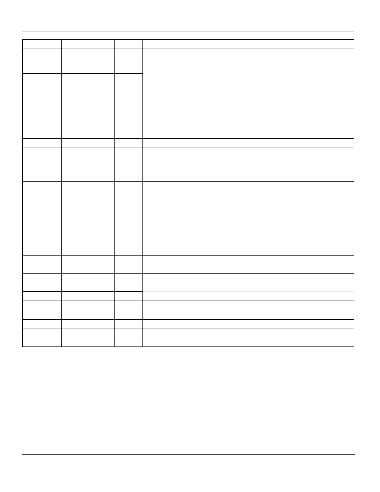
Pin Number
51
Pin Name
MDIO
Type(1)
Ipu/O
52
COL
O
53
INT_N
O
54
DVDDL
P
55
CLK125_NDO /
I/O
LED_MODE
56
RESET_N
Ipu
57
TX_CLK
O
58
LDO_O
O
59
AVDDL_PLL
P
60
XO
O
61
XI
I
62
AVDDH
P
63
ISET
I/O
64
AGNDH
Gnd
PADDLE
P_GND
Gnd
Note:
1. P = Power supply.
Gnd = Ground.
I = Input.
O = Output.
I/O = Bi-directional.
Ipu = Input with internal pull-up.
Ipu/O = Input with internal pull-up / Output.
Pin Function
Management Data Input / Output
This pin is synchronous to MDC (pin 50) and requires an external pull-up resistor
to DVDDH (digital VDD) in a range from 1.0KΩ to 4.7KΩ.
GMII Mode:
GMII COL (Collision Detected) Output
MII Mode:
MII COL (Collision Detected) Output
Interrupt Output
This pin provides a programmable interrupt output and requires an external pull-up
resistor to DVDDH (digital VDD) in a range from 1.0KΩ to 4.7KΩ when active low.
Register 1Bh is the Interrupt Control/Status Register for programming the interrupt
conditions and reading the interrupt status. Register 1Fh bit 14 sets the interrupt
output to active low (default) or active high.
1.2V digital VDD
125MHz Clock Output
This pin provides a 125MHz reference clock output option for use by the MAC. /
Config Mode:
The pull-up/pull-down value is latched as LED_MODE during
power-up / reset. See “Strapping Options” section for details.
Chip Reset (active low)
Hardware pin configurations are strapped-in at the de-assertion (rising edge) of
RESET_N. See “Strapping Options” section for more details.
MII Mode:
MII TX_CLK (Transmit Reference Clock) Output
On-chip 1.2V LDO Controller Output
This pin drives the input gate of a P-channel MOSFET to generate 1.2V for the
chip’s core voltages. If 1.2V is provided by the system and this pin is not used, it
can be left floating.
1.2V analog VDD for PLL
25MHz Crystal feedback
This pin is a no connect if oscillator or external clock source is used.
Crystal / Oscillator / External Clock Input
25MHz +/-50ppm tolerance
3.3V analog VDD
Set transmit output level
Connect a 4.99KΩ 1% resistor to ground on this pin.
Analog ground
Exposed Paddle on bottom of chip
Connect P_GND to ground.
September 2010
13
M9999-091010-1.1
Share Link: 