KSZ9021RL Ver la hoja de datos (PDF) - Micrel
Número de pieza
componentes Descripción
Fabricante
KSZ9021RL Datasheet PDF : 59 Pages
| |||
Micrel, Inc.
KSZ9021RL/RN
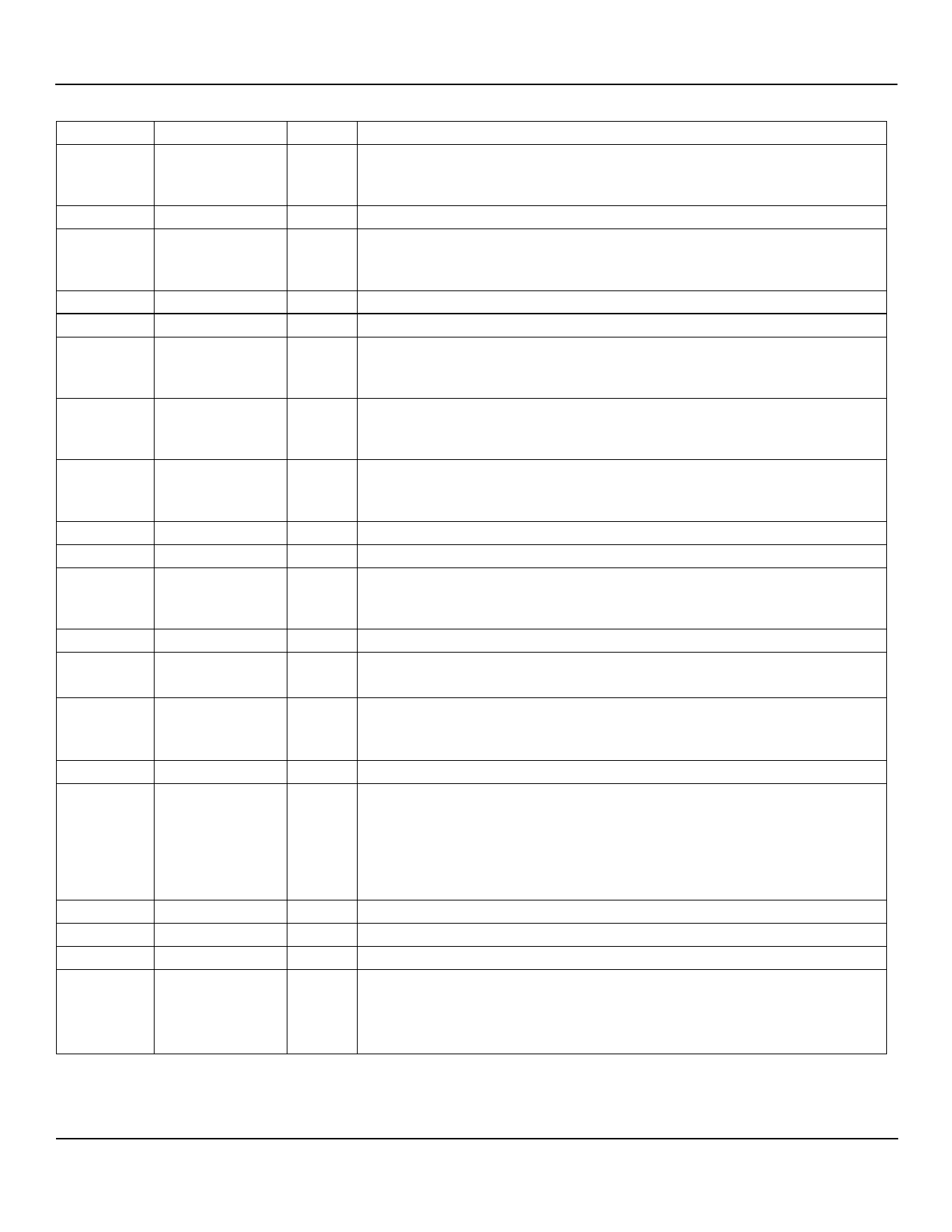
Pin Number
36
37
38
39
40
41
42
43
44
45
46
47
48
Pin Name
RXD3 /
MODE3
DVDDH
RXD2 /
MODE2
VSS
DVDDL
RXD1 /
MODE1
RXD0 /
MODE0
RX_DV /
CLK125_EN
DVDDH
RX_ER
RX_CLK /
PHYAD2
CRS
MDC
49
MDIO
50
COL
51
INT_N
52
DVDDL
53
VSS
54
DVDDL
55
CLK125_NDO /
LED_MODE
Type(1)
I/O
P
I/O
Gnd
P
I/O
I/O
I/O
P
O
I/O
O
Ipu
Ipu/O
O
O
P
Gnd
P
I/O
Pin Function
RGMII Mode: RGMII RD3 (Receive Data 3) Output /
Config Mode: The pull-up/pull-down value is latched as MODE3 during
power-up/reset. See “Strapping Options” section for details.
3.3V/2.5V digital VDD
RGMII Mode: RGMII RD2 (Receive Data 2) Output /
Config Mode: The pull-up/pull-down value is latched as MODE2 during
power-up/reset. See “Strapping Options” section for details.
Digital ground
1.2V digital VDD
RGMII Mode: RGMII RD1 (Receive Data 1) Output /
Config Mode: The pull-up/pull-down value is latched as MODE1 during
power-up/reset. See “Strapping Options” section for details.
RGMII Mode: RGMII RD0 (Receive Data 0) Output /
Config Mode: The pull-up/pull-down value is latched as MODE0 during
power-up/reset. See “Strapping Options” section for details.
RGMII Mode: RGMII RX_CTL (Receive Control) Output /
Config Mode: Latched as CLK125_NDO Output Enable during power-up/reset.
See “Strapping Options” section for details.
3.3V/2.5V digital VDD
RGMII Mode: This pin is not used and should be left as a no connect.
RGMII Mode: RGMII RXC (Receive Reference Clock) Output /
Config Mode: The pull-up/pull-down value is latched as PHYAD[2] during
power-up/reset. See “Strapping Options” section for details.
RGMII Mode: This pin is not used and should be left as a no connect.
Management Data Clock Input
This pin is the input reference clock for MDIO (pin 49).
Management Data Input/Output
This pin is synchronous to MDC (pin 48) and requires an external pull-up resistor
to 3.3V/2.5V digital VDD in a range from 1.0kΩ to 4.7kΩ.
RGMII Mode: This pin is not used and should be left as a no connect.
Interrupt Output
This pin provides a programmable interrupt output and requires an external pull-up
resistor to 3.3V/2.5V digital VDD in a range from 1.0kΩ to 4.7kΩ when active low.
Register 1Bh is the Interrupt Control/Status Register for programming the interrupt
conditions and reading the interrupt status. Register 1Fh bit 14 sets the interrupt
output to active low (default) or active high.
1.2V digital VDD
Digital ground
1.2V digital VDD
125MHz Clock Output
This pin provides a 125MHz reference clock output option for use by the MAC. /
Config Mode: The pull-up/pull-down value is latched as LED_MODE during
power-up/reset. See “Strapping Options” section for details.
February 13, 2014
12
Revision 1.2
Share Link: 