NCS2202SQ1T2G Ver la hoja de datos (PDF) - ON Semiconductor
Número de pieza
componentes Descripción
Fabricante
NCS2202SQ1T2G
ON Semiconductor

NCS2202SQ1T2G Datasheet PDF : 20 Pages
| |||
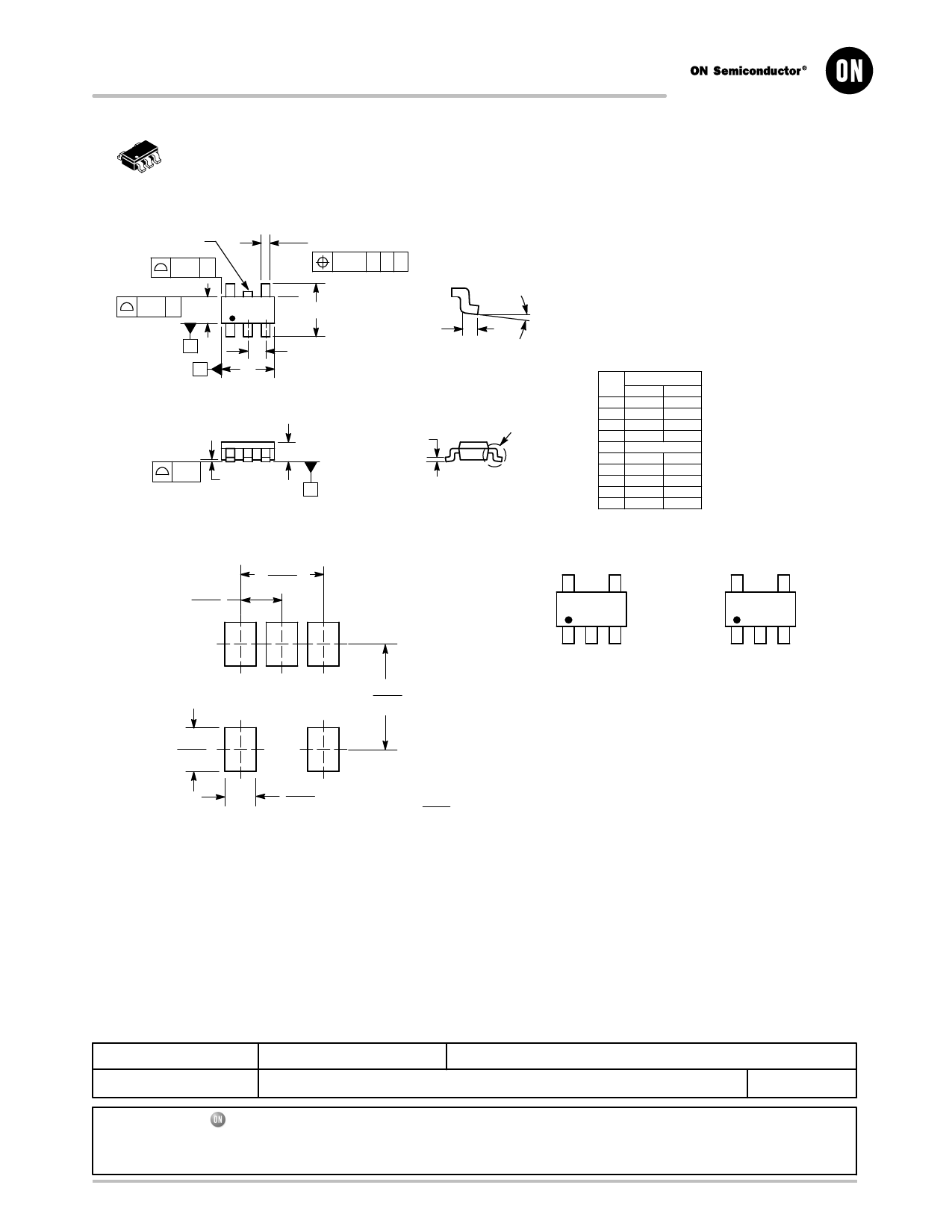
MECHANICAL CASE OUTLINE
PACKAGE DIMENSIONS
5
1
SCALE 2:1
TSOP−5
CASE 483
ISSUE N
NOTE 5
2X 0.10 T
2X
0.20 T B 5
4
1 23
B
G
A
A
TOP VIEW
D 5X
0.20 C A B
S
M
K
DETAIL Z
C
0.05
H
SIDE VIEW
C
SEATING
PLANE
DETAIL Z
J
END VIEW
DATE 12 AUG 2020
NOTES:
1. DIMENSIONING AND TOLERANCING PER ASME
Y14.5M, 1994.
2. CONTROLLING DIMENSION: MILLIMETERS.
3. MAXIMUM LEAD THICKNESS INCLUDES LEAD FINISH
THICKNESS. MINIMUM LEAD THICKNESS IS THE
MINIMUM THICKNESS OF BASE MATERIAL.
4. DIMENSIONS A AND B DO NOT INCLUDE MOLD
FLASH, PROTRUSIONS, OR GATE BURRS. MOLD
FLASH, PROTRUSIONS, OR GATE BURRS SHALL NOT
EXCEED 0.15 PER SIDE. DIMENSION A.
5. OPTIONAL CONSTRUCTION: AN ADDITIONAL
TRIMMED LEAD IS ALLOWED IN THIS LOCATION.
TRIMMED LEAD NOT TO EXTEND MORE THAN 0.2
FROM BODY.
MILLIMETERS
DIM MIN MAX
A 2.85 3.15
B 1.35 1.65
C 0.90 1.10
D 0.25 0.50
G
0.95 BSC
H 0.01 0.10
J 0.10 0.26
K 0.20 0.60
M
0 _ 10 _
S 2.50 3.00
SOLDERING FOOTPRINT*
0.95
0.037
1.9
0.074
2.4
0.094
1.0
0.039
0.7
0.028
ǒ Ǔ SCALE 10:1
mm
inches
*For additional information on our Pb−Free strategy and soldering
details, please download the ON Semiconductor Soldering and
Mounting Techniques Reference Manual, SOLDERRM/D.
GENERIC
MARKING DIAGRAM*
5
XXXAYWG
G
1
Analog
5
XXX MG
G
1
Discrete/Logic
XXX = Specific Device Code
A = Assembly Location
Y = Year
W = Work Week
G = Pb−Free Package
XXX = Specific Device Code
M = Date Code
G = Pb−Free Package
(Note: Microdot may be in either location)
*This information is generic. Please refer to
device data sheet for actual part marking.
Pb−Free indicator, “G” or microdot “ G”,
may or may not be present.
DOCUMENT NUMBER: 98ARB18753C
DESCRIPTION: TSOP−5
Electronic versions are uncontrolled except when accessed directly from the Document Repository.
Printed versions are uncontrolled except when stamped “CONTROLLED COPY” in red.
PAGE 1 OF 1
ON Semiconductor and
are trademarks of Semiconductor Components Industries, LLC dba ON Semiconductor or its subsidiaries in the United States and/or other countries.
ON Semiconductor reserves the right to make changes without further notice to any products herein. ON Semiconductor makes no warranty, representation or guarantee regarding
the suitability of its products for any particular purpose, nor does ON Semiconductor assume any liability arising out of the application or use of any product or circuit, and specifically
disclaims any and all liability, including without limitation special, consequential or incidental damages. ON Semiconductor does not convey any license under its patent rights nor the
rights of others.
© Semiconductor Components Industries, LLC, 2018
www.onsemi.com
Share Link: