LC5824 Ver la hoja de datos (PDF) - SANYO -> Panasonic
Número de pieza
componentes Descripción
Fabricante
LC5824 Datasheet PDF : 24 Pages
| |||
LC5824, LC5823, LC5822
Continued from preceding page.
Pin No.
Pin
32
SO1
33
SO2
34
SO3
35
SO4
31
ALM
40
RES
44
Seg 22
64
Seg 21
1
Seg 22
21
Seg 42
65
COM1
66
COM2
79
COM3
80
COM4
41
TST
—
TEST
—
TEST
I/O
Function
I/O port
• Input pins used to acquire input data to RAM.
• Output pins used to output RAM data.
• Pull-down resistors are built in.
SO1 to SO3 are also used as the serial interface pins.
• The serial interface function can be selected under program
I/O
control.
• Pin functions:
SO1: Serial input
SO2: Serial output
SO3: Serial clock
The serial clock can be taken from either internal or external
sources, and can be set up to detect either rising or falling
edges under program control.
Output-only pin
Output • A signal modulated by ø0, ø3, or ø4 can be output under
program control.
Options
Identical to M1 through
M4
Status at reset
Identical to M1 through
M4
Low-level output
Input
IC internal reset input
• The program counter is set to point to location 00H.
• The reset input level can be set to be either high or low.
• Either a pull-up or a pull-down resistor is built in.
Note: Applications must apply the reset signal level for at least
500 µs to effect a reset.
• Selection of a pull-up or
pull-down resistor
• Selection of active-low
or active-high reset
logic
Output
LCD panel drive outputs/general-purpose outputs
• LCD panel drive
(1) Static
(2) 1/2 bias 1/2 duty
(3) 1/2 bias 1/3 duty
(4) 1/2 bias 1/4 duty
(5) 1/3 bias 1/3 duty
(6) 1/3 bias 1/4 duty
One of items (1) through (5) is selected as a mask option.
• General-purpose output ports
(1) CMOS output
(2) p-channel open-drain output
(3) n-channel open-drain output
One of items (1) through (3) is selected as a mask option.
• The adoption of the segment PLA in these microcontrollers
means that there is no need for programs to control the
LCD/general-purpose output states of these pins.
• Output latch control is supported in the oscillator stopped
standby states and during a reset.
• Any combination of LCD and general-purpose output functions
may be used.
• Switching between LCD
drive output and
general-purpose output
• Switching between the
LCD drive type options
—Static
—1/2 bias 1/2 duty
—1/2 bias 1/3 duty
—1/2 bias 1/4 duty
—1/3 bias 1/3 duty
—1/3 bias 1/4 duty
• General-purpose output
type switching
—CMOS
—p-channel open-drain
—n-channel open-drain
• Standby mode output
latch control
• When used for LCD
drive:
—All lit
—All off
* Determined by the
master options
• When used as general-
purpose outputs:
—High level
—Low level
* Determined by the
master options
Note: When a
combination of LCD drive
and general-purpose
outputs is selected, these
pins will be either:
All lit/high-level output, or
All off/low-level output.
• During the reset period,
the LCD drive functions
as static drive.
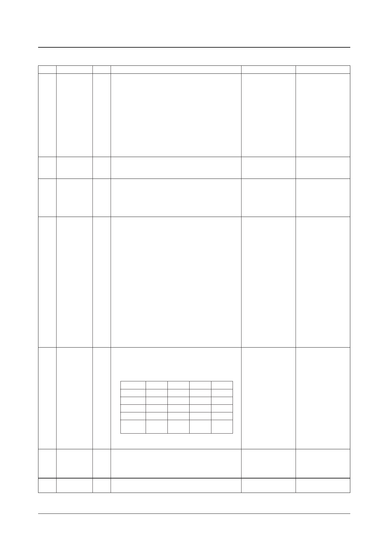
Common drive outputs for the LCD panel
The table below lists which pins are used in each of the drive
types.
However, note that the listed alternation frequencies are the
typical specifications when ø0 is 32.768 kHz.
Output
COM1
COM2
COM3
COM4
Alternation
frequency
Static
q
!
!
!
32 Hz
1/2 duty
q
q
!
!
1/3 duty
q
q
q
!
1/4/duty
q
q
q
q
32 Hz 42.7 Hz 64 Hz
Note: Note that the “!” symbol indicates that the corresponding
common pin cannot be used in that drive type.
* In products with the CF
specifications, the
alternation frequency
signal stops briefly.
Input
Test input
• In the QIP-80 version, this pin must be connected to VSS.
• In the chip version, this pin must be left open or connected to
VSS.
— Test pins.
— (These are not used in the device user interface.)
No. 5944-7/24
Share Link: 