TDA8160 Ver la hoja de datos (PDF) - STMicroelectronics
Número de pieza
componentes Descripción
Fabricante
TDA8160 Datasheet PDF : 4 Pages
| |||
TDA8160
ABSOLUTE MAXIMUM RATINGS
Symbol
Vs
Tstg–j
Ptot
Parameter
Supply Voltage
Storage and Junction Temperature
Total Power Dissipation at Tamb = 70 °C
Value
Unit
16
V
– 40, +150
°C
400
mW
THERMAL DATA
Symbol
Parameter
Rth (j-a) Thermal Resistance Junction-ambient
Value
Unit
Max
200
°C/W
ELECTRICAL CHARACTERISTICS
(Refer to the test circuit ; VS = 5V, fO = 10kHz, Tamb = 25oC, unless otherwise specified)
Symbol
VS
IS
V3
GV 1st
gm 2nd
VIN
IIN
RIN
LfR
N
Parameter
Supply Voltage
Supply Current (Pin 3)
Stabilized Voltage at Pin 3
Voltage Gain (1st stage)
Transconductance (2nd stage)
Input Voltage Sensitivity (Pin 5)
Input Current Sensitivity (Pin 5)
Input Impedance
Low Frequency Rejection at the Input
Stage
Noise Signal at Pin 7
Test Conditions
Applied between Pins 3 and 6
I3 = 8mA
For Full Swing at the Output Pin 1
Rgen = 600Ω
For Full Swing at the Output Pin 1
C1 = 100pF , f = 100HZ
C4 Missing
Min.
4
Typ.
5
6
5.5
28
15
2
10
200
Max.
5.25
30
200
Unit
V
mA
V
dB
mA/V
mVP
nAP
kΩ
dB
mVPP
CIRCUIT DESCRIPTION (see the block diagram)
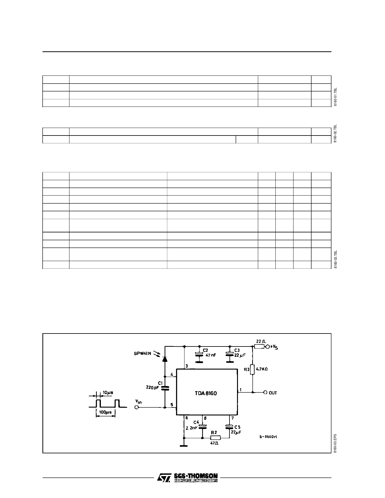
The infrared light received from D1 generates an
AC signal that comes in to the device at pin 5. The
capacitor C1 and the integrated 10kΩ resistor
(pin 4) filter out the low frequency noise.
TEST CIRCUIT
The first stage shows a voltage gain of about 28dB ;
the second stage is a voltage to current converter
of 50mA/V (R2 = Zero). A sensitive peak detector
detects the amplifier signal ; one open collector
output (pin 1) gives out the recovered pulses.
2/4
Share Link: 