TLV4946-2L Ver la hoja de datos (PDF) - Infineon Technologies
Número de pieza
componentes Descripción
Fabricante
TLV4946-2L
Infineon Technologies

TLV4946-2L Datasheet PDF : 16 Pages
| |||
2
Functional Description
TLV4946-2L
Functional Description
2.1
General
Precise magnetic switching thresholds and high temperature stability are achieved by active compensation circuits
and chopper techniques on chip. Offset voltages generated by temperature-induced stress or overmolding are
canceled so that high accuracy is achieved. The IC has an open collector output stage with 20 mA current sink
capability. A wide operating voltage range from 2.7 V to 18 V with reverse polarity protection down to -18 V makes
the TLV4946-2L suitable for a wide range of applications. A magnetic south pole with a field strength above Bop
turns the output on. A magnetic north pole exceeding Brp turns it off.
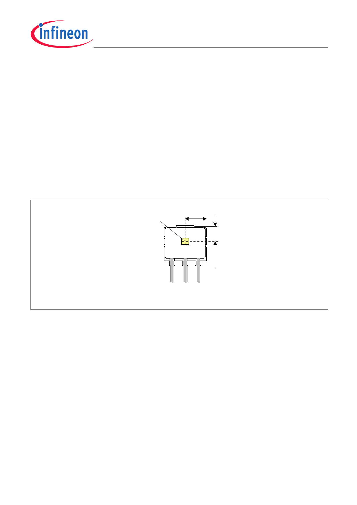
2.2
Pin Configuration
Center of
Sensitive Area
2.08 ± 0.1
1.35 ± 0.1
12 3
PG-SSO-3-2
Figure 1 Pin Configuration and sensitive area (Top view, figure not to scale)
Datasheet
8
Rev1.1, 2010-08-02
Share Link: