MAX6133BASA50 Ver la hoja de datos (PDF) - Maxim Integrated
NГәmero de pieza
componentes DescripciГіn
Fabricante
MAX6133BASA50 Datasheet PDF : 13 Pages
| |||
3ppm/В°C, Low-Power, Low-Dropout
Voltage Reference
ABSOLUTE MAXIMUM RATINGS
Voltage (with Respect to GND)
IN ........................................................................-0.3V to +13V
OUT..............................................-0.3V to +6V or (VIN + 0.3V)
OUT Short Circuit to IN or GND Duration ...............................60s
Continuous Power Dissipation (TA = +70В°C)
8-Pin ВөMAX (derate 5.5mW/В°C above +70В°C) .............362mW
8-Pin SO (derate 5.88mW/В°C above +70В°C)................471mW
Operating Temperature Range .........................-40В°C to +125В°C
Storage Temperature Range .............................-65В°C to +150В°C
Junction Temperature ......................................................+150В°C
Lead Temperature (soldering, 10s) .................................+300В°C
Stresses beyond those listed under вҖңAbsolute Maximum RatingsвҖқ may cause permanent damage to the device. These are stress ratings only, and functional
operation of the device at these or any other conditions beyond those indicated in the operational sections of the specifications is not implied. Exposure to
absolute maximum rating conditions for extended periods may affect device reliability.
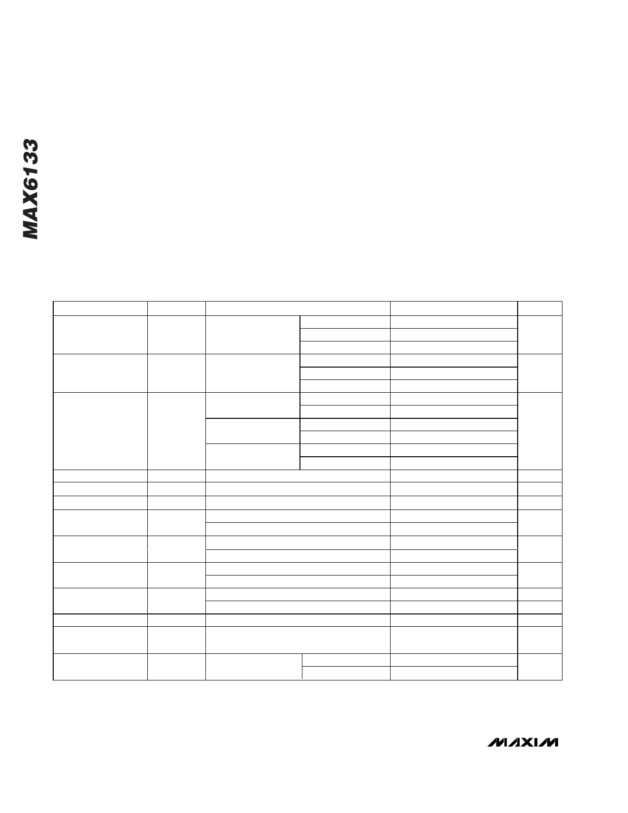
ELECTRICAL CHARACTERISTICSвҖ”MAX6133_25 (VOUT = 2.500V)
(VIN = 5V, CLOAD = 0.1ВөF, IOUT = 0, TA = TMIN to TMAX. Typical values are at TA = +25В°C, unless otherwise noted.)
PARAMETER
Output Voltage
Output Voltage
Accuracy
Output Voltage
Temperature
Coefficient (Note 1)
Input Voltage Range
Line Regulation
Load Regulation
Dropout Voltage
(Note 2)
Quiescent Supply
Current
Output Short-Circuit
Current
Output Voltage Noise
Turn-On Settling Time
Thermal Hysteresis
(Note 3)
Long-Term Stability
SYMBOL
CONDITIONS
A grade SO
VOUT
TA = +25В°C
B grade SO
ВөMAX
A grade SO
TA = +25В°C
B grade SO
ВөMAX
A grade SO
TCVOUT B grade SO
ВөMAX
TA = -40В°C to +85В°C
TA = -40В°C to +125В°C
TA = -40В°C to +85В°C
TA = -40В°C to +125В°C
TA = -40В°C to +85В°C
TA = -40В°C to +125В°C
VIN
Inferred from line regulation
вҲҶVOUT/вҲҶVIN 2.7V вүӨ VIN вүӨ 12.6V
вҲҶVOUT/вҲҶIOUT -100ВөA вүӨ IOUT вүӨ 15mA
VDO
вҲҶVOUT = 0.1%, IOUT = 1mA
вҲҶVOUT = 0.1%, IOUT = 10mA
IIN
TA = +25В°C
TA = -40В°C to +125В°C
ISC
Short to GND: VOUT = 0V
Short to VIN: VOUT = VIN
0.1Hz вүӨ f вүӨ 10Hz
en
10Hz вүӨ f вүӨ 1kHz
tON
VOUT settles to Вұ0.01% of final value
вҲҶt = 1000 hours
SO
ВөMAX
MIN
2.4990
2.4980
2.4985
-0.04
-0.08
-0.06
2.7
TYP
2.5000
2.5000
2.5000
1
4
3
5
1
2
2
0.003
0.02
0.2
40
90
-2
16
12
500
120
40
145
MAX
2.5010
2.5020
2.5015
+0.04
+0.08
+0.06
3
7
5
10
5
7
12.6
30
0.05
0.2
0.4
60
85
UNITS
V
%
ppm/В°C
V
ВөV/V
mV/mA
V
ВөA
mA
ВөVP-P
ВөVRMS
Вөs
ppm
ppm
2 _______________________________________________________________________________________
Share Link: 