ISL3034E Ver la hoja de datos (PDF) - Intersil
Número de pieza
componentes Descripción
Fabricante
ISL3034E Datasheet PDF : 16 Pages
| |||
ISL3034E, ISL3035E, ISL3036E
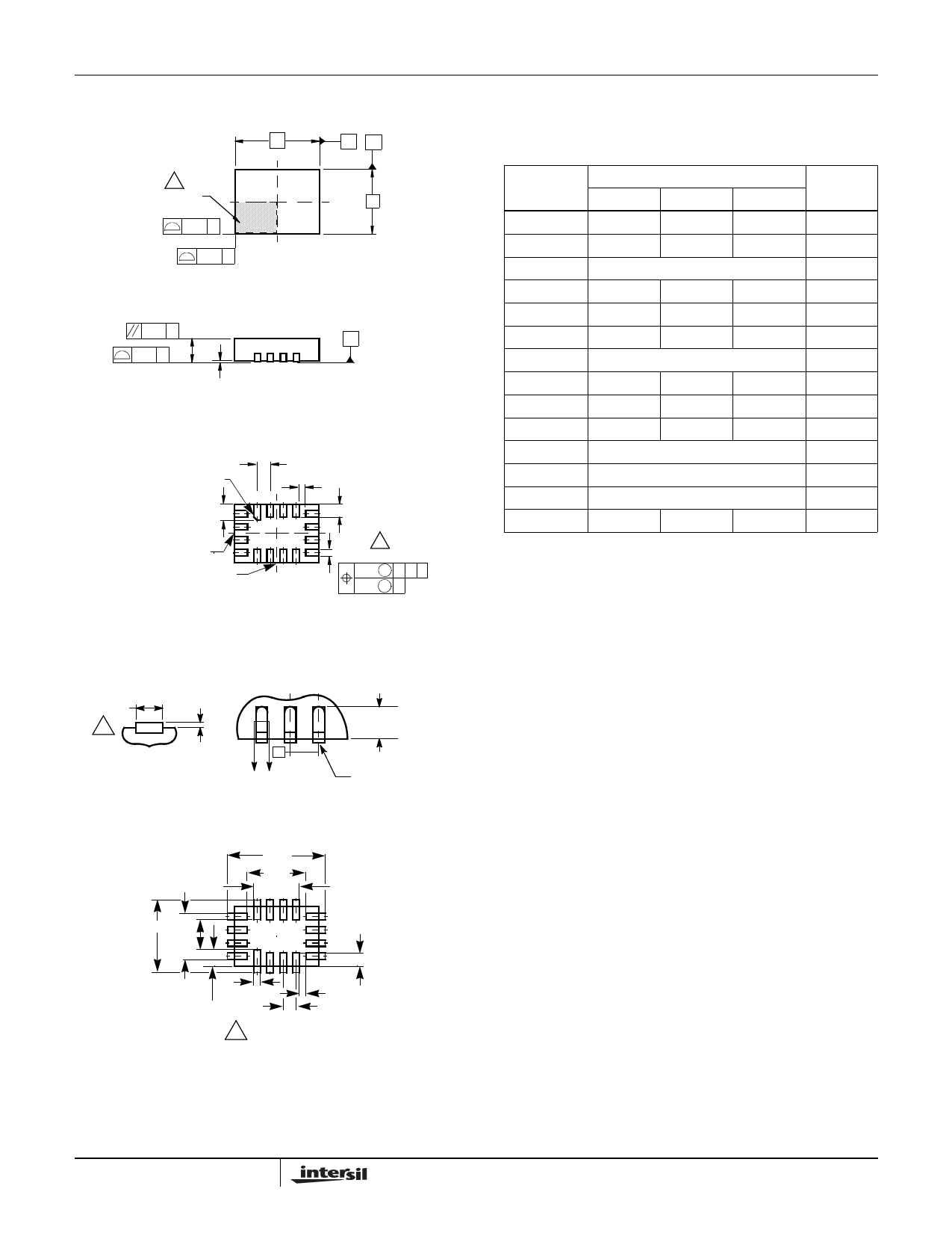
Ultra Thin Quad Flat No-Lead Plastic Package (UTQFN)
D
6
INDEX AREA N
2X 0.10 C
12
2X 0.10 C
TOP VIEW
AB
E
0.10 C
C
0.05 C
A
SEATING PLANE
A1
SIDE VIEW
e
PIN #1 ID
12
L1
K
NX L
(DATUM B)
(DATUM A)
NX b 5
16X
0.10 M C A B
0.05 M C
BOTTOM VIEW
NX (b)
(A1)
5
SECTION "C-C"
CL
e
CC
L
TERMINAL TIP
L16.2.6x1.8A
16 LEAD ULTRA THIN QUAD FLAT NO-LEAD PLASTIC PACKAGE
MILLIMETERS
SYMBOL
MIN NOMINAL MAX
NOTES
A
0.45
0.50
0.55
-
A1
-
-
0.05
-
A3
0.127 REF
-
b
0.15
0.20
0.25
5
D
2.55
2.60
2.65
-
E
1.75
1.80
1.85
-
e
0.40 BSC
-
K
0.15
-
-
-
L
0.35
0.40
0.45
-
L1
0.45
0.50
0.55
-
N
16
2
Nd
4
3
Ne
4
3
θ
0
-
12
4
NOTES:
Rev. 5 2/09
1. Dimensioning and tolerancing conform to ASME Y14.5-1994.
2. N is the number of terminals.
3. Nd and Ne refer to the number of terminals on D and E side,
respectively.
4. All dimensions are in millimeters. Angles are in degrees.
5. Dimension b applies to the metallized terminal and is measured
between 0.15mm and 0.30mm from the terminal tip.
6. The configuration of the pin #1 identifier is optional, but must be
located within the zone indicated. The pin #1 identifier may be
either a mold or mark feature.
7. Maximum package warpage is 0.05mm.
8. Maximum allowable burrs is 0.076mm in all directions.
9. JEDEC Reference MO-255.
10. For additional information, to assist with the PCB Land Pattern
Design effort, see Intersil Technical Brief TB389.
3.00
1.80
1.40
1.40
2.20
0.90
0.40
0.20
0.20
0.50
0.40
10 LAND PATTERN
14
FN6492.0
March 31, 2009
Share Link: 