FD2000 Ver la hoja de datos (PDF) - Unspecified
Número de pieza
componentes Descripción
Fabricante
FD2000 Datasheet PDF : 37 Pages
| |||

FD2000
Rev1.0
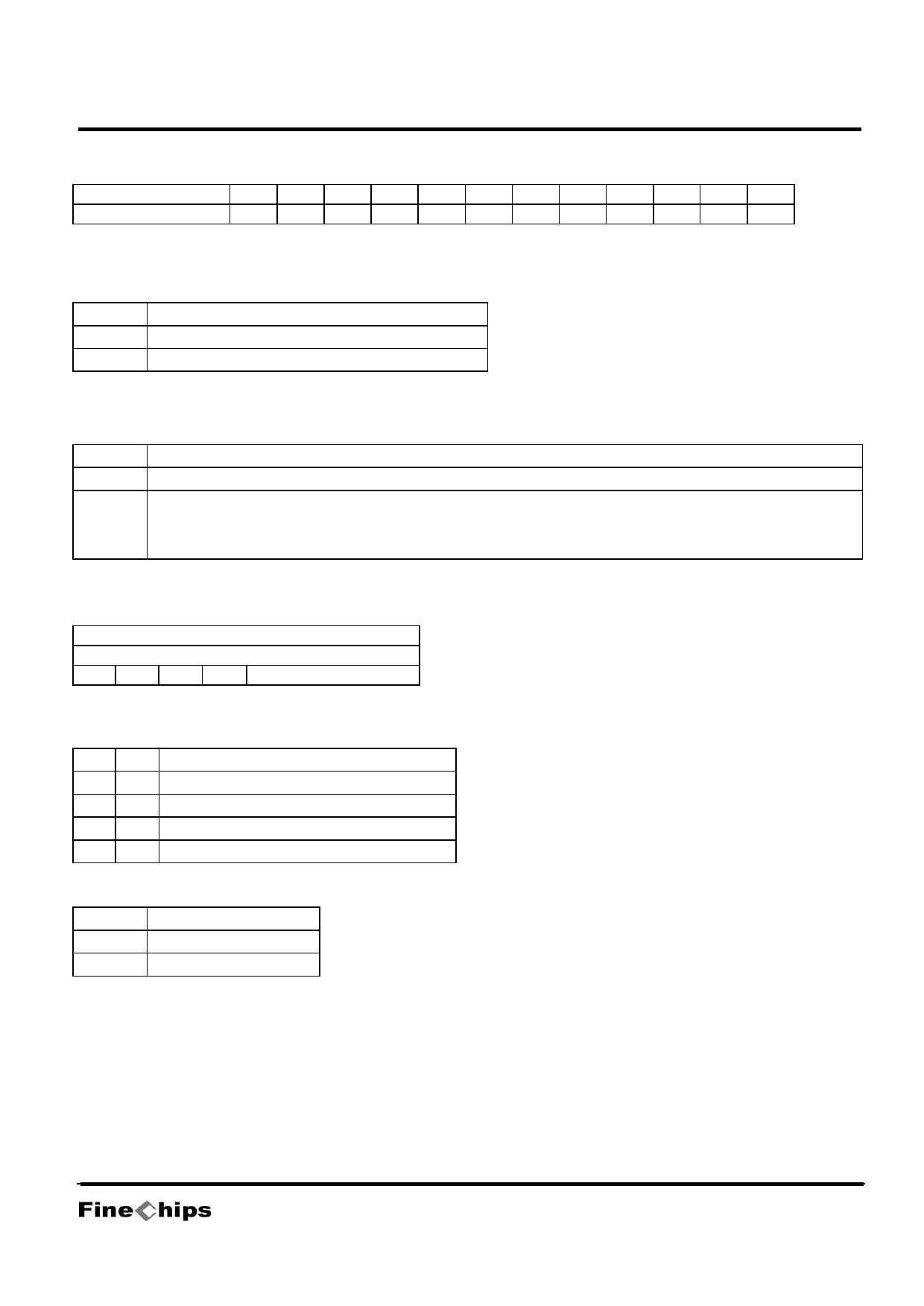
10.2.2. DG1 to DG12: Specifies the display digit
Display digit
1
2
3
4
5
6
7
8
9
10
11
12
Display digit data
DG1 DG2 DG3 DG4 DG5 DG6 DG7 DG8 DG9 DG10 DG11 DG12
For example, if DG1 to DG6 are 1, and DG7 to DG12 are 0, then display digits 1 to 6 will be turned on, and display digits 7 to 12
will be turned off (blanked).
10.2.3. SC: Controls the common and segment output pins
SC
Common and segment output pin states
0
Output of LCD drive waveforms
1
Fixed at the VSS level (all segments off)
NOTE: When SC is 1, the S1 to S60 and COM1 to COM10 output pins are set to the VSS level, regardless of the M, A, and DG1 to DG12
data.
10.2.4. BU: Controls the normal mode and power saving mode
BU
Mode
0
Normal mode
Power saving mode
1
(In this mode, the OSCI and OSCO pins oscillator is stopped, and the common and segment pins are set to the VSS level. In
this mode, instructions other than the “display on/off control” instruction cannot be executed. Thus applications must set the LSI
to normal mode before executing any of the other instructions.)
10.3. DISPLAY SHIFT ― Shifts the display
Code
D56 D57 D58 D59 D60 D61 D62 D63
M
A R/L X
0
0
1
1
X: don’t care
10.3.1. M, A: Specifies the data to be shifted
M
A
Shift operating state
0
0 Neither MDATA nor ADATA is shifted
0
1 Only ADATA is shifted
1
0 Only MDATA is shifted
1
1 Both MDATA and ADATA are shifted
10.3.2. R/L: Shift direction specification
R/L
Shift direction
0
Left shift
1
Right shift
16/37