ADSP-2186 Ver la hoja de datos (PDF) - Analog Devices
Número de pieza
componentes Descripción
Fabricante
ADSP-2186 Datasheet PDF : 36 Pages
| |||
ADSP-2186
Parameter
Min
Max
Unit
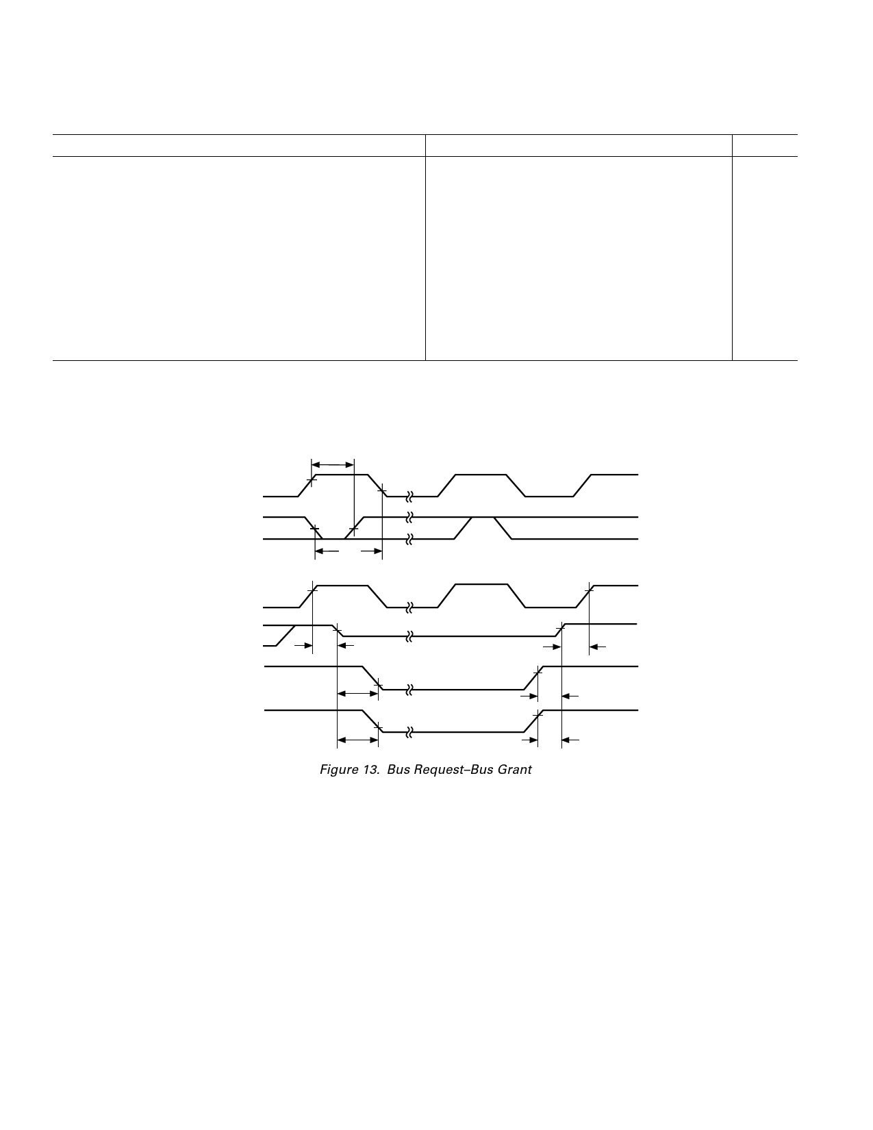
Bus Request–Bus Grant
Timing Requirements:
tBH
BR Hold after CLKOUT High1
tBS
BR Setup before CLKOUT Low1
Switching Characteristics:
tSD
CLKOUT High to xMS, RD, WR Disable
tSDB
xMS, RD, WR Disable to BG Low
tSE
BG High to xMS, RD, WR Enable
tSEC
xMS, RD, WR Enable to CLKOUT High
tSDBH
xMS, RD, WR Disable to BGH Low2
tSEH
BGH High to xMS, RD, WR Enable2
0.25 tCK + 2
ns
0.25 tCK + 17
ns
0.25 tCK + 10
ns
0
ns
0
ns
0.25 tCK – 7
ns
0
ns
0
ns
NOTES
xMS = PMS, DMS, CMS, IOMS, BMS.
1BR is an asynchronous signal. If BR meets the setup/hold requirements, it will be recognized during the current clock cycle; otherwise the signal will be recognized on
the following cycle. Refer to the ADSP-218x DSP Hardware Reference, for BR/BG cycle relationships.
2BGH is asserted when the bus is granted and the processor requires control of the bus to continue.
tBH
CLKOUT
BR
tBS
CLKOUT
PMS, DMS
BMS, RD
WR
BG
BGH
tSD
tSEC
tSDB
tSE
tSDBH
tSEH
Figure 13. Bus Request–Bus Grant
–18–
REV. B
Share Link: 