DS2409P-TU0026R Ver la hoja de datos (PDF) - Maxim Integrated
Número de pieza
componentes Descripción
Fabricante
DS2409P-TU0026R Datasheet PDF : 18 Pages
| |||
DS2409
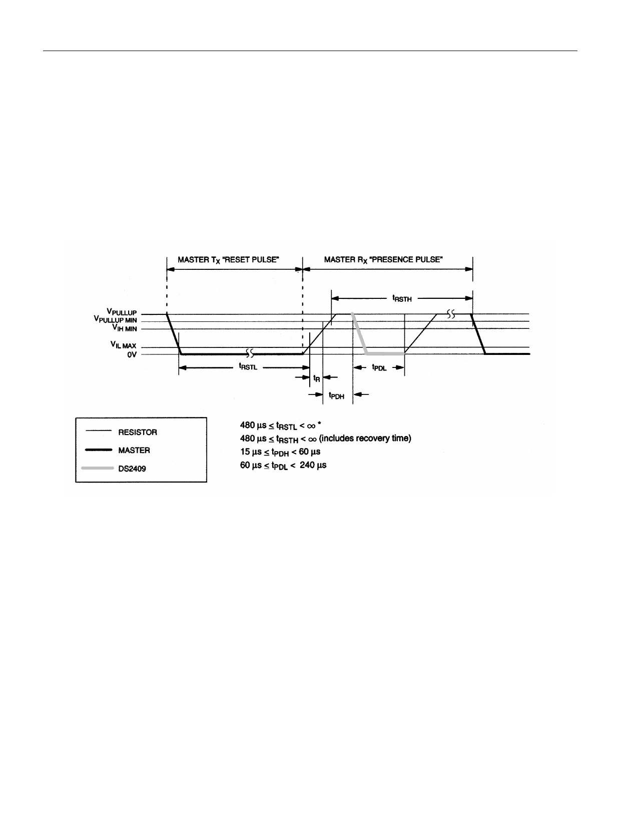
1-WIRE SIGNALING
The DS2409 requires strict protocols to ensure data integrity. The protocol consists of four types of
signaling on one line: Reset Sequence with Reset Pulse and Presence Pulse, Write 0, Write 1 and Read
Data. All these signals except presence pulse are initiated by the bus master. The initialization sequence
required to begin any communication with the DS2409 is shown in Figure 8. A reset pulse followed by a
presence pulse indicates the DS2409 is ready to send or receive data given the correct ROM command
and control function command. The bus master transmits (TX) a reset pulse (tRSTL, minimum 480 µs).
The bus master then releases the line and goes into receive mode (RX). The 1-Wire bus is pulled to a high
state via the pullup resistor. After detecting the rising edge on the data line, the DS2409 waits (tPDH, 15-60
µs) and then transmits the presence pulse (tPDL, 60-240 µs).
INITIALIZATION PROCEDURE “RESET AND PRESENCE PULSES” Figure 8
*In order not to mask interrupt signaling by other devices on the 1-Wire bus, tRSTL + tR should always be
less than 960 µs.
**The slew rate of the Presence Pulse is actively limited by the DS2409 to 1V/µs typically to minimize
ringing. The slope of all other edges is controlled by the 1-Wire bus driver at the host.
READ/WRITE TIME SLOTS
The definitions of write and read time slots are illustrated in Figure 9. All time slots are initiated by the
master driving the data line low. The falling edge of the data line synchronizes the DS2409 to the master
by triggering a delay circuit in the DS2409. During write time slots, the delay circuit determines when the
DS2409 will sample the data line. For a read data time slot, if a “0” is to be transmitted, the delay circuit
determines how long the DS2409 will hold the data line low overriding the 1 generated by the master. If
the data bit is a “1”, the device will leave the read data time slot unchanged.
12 of 18
102199
Share Link: 