YDA142 Ver la hoja de datos (PDF) - Yamaha Corporation
Número de pieza
componentes Descripción
Fabricante
YDA142 Datasheet PDF : 18 Pages
| |||
YDA142
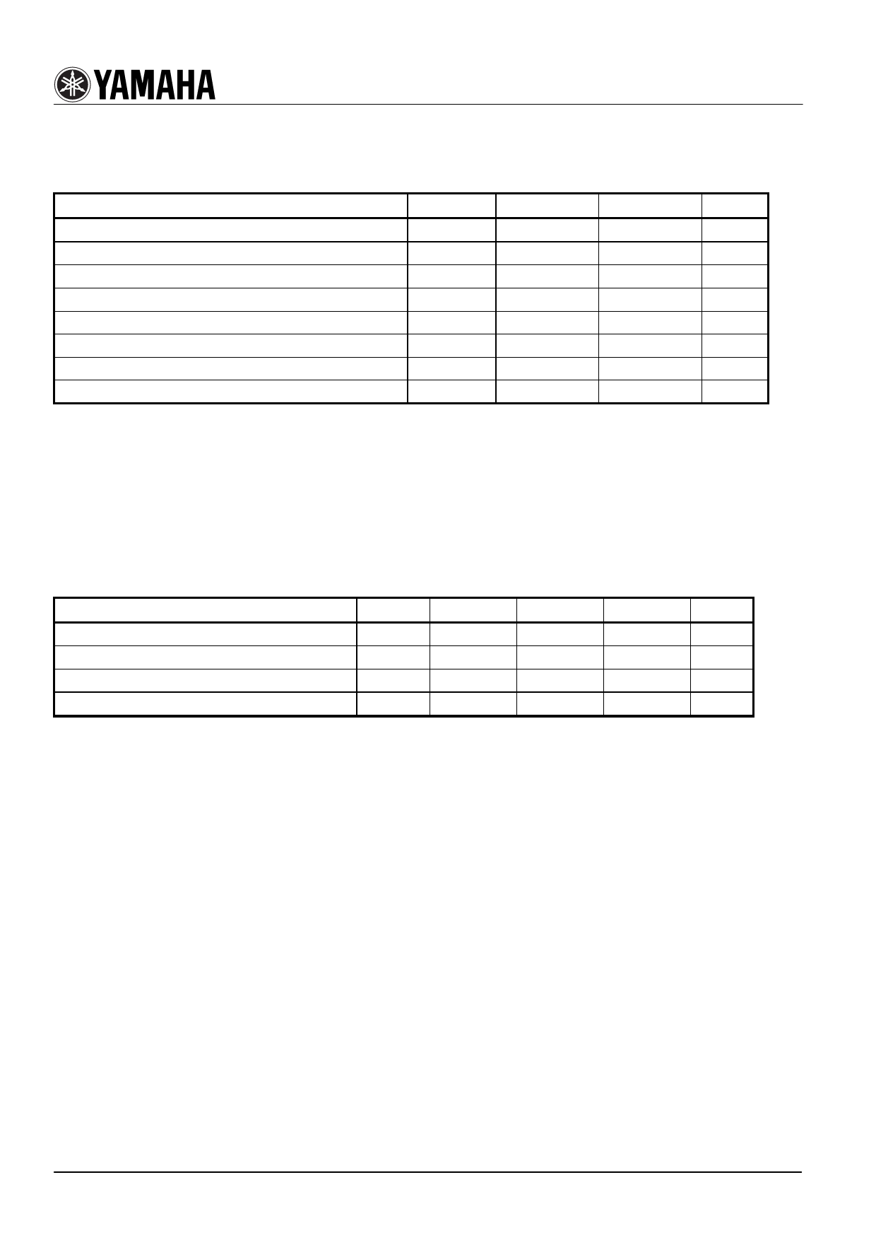
■Electrical characteristics
●Absolute Maximum Ratings Note 6)
Item
Symbol
Min.
Max.
Unit
Power Supply Terminal (VDDP) voltage range Note 1,2,3)
VDDP
-0.3
14.0
V
SLEEPN, PROTN terminal voltage range
Control line terminal voltage range Note 4)
Input/Output terminal voltage range Note 5)
VIN1
VIN3
VIN4
VSS-0.3
VDDP+0.3
V
VSS-0.3
VREG+0.3
V
VSS-0.3
VREG+0.3
V
Power Dissipation (Ta=25℃, 4-layer board)
PD25
6.4
W
Power Dissipation (Ta=70℃, 4-layer board)
PD70
3.6
W
Junction Temperature
TJMAX
125
℃
Storage Temperature
TSTG
-50
125
℃
Note 1) VSS means AVSS, VSSBGR, DVSS, PVSSR, and PVSSL. Keep all the VSS terminals at the same potential.
Note 2) The voltage is based on VSS=0V.
Note 3) The power supply terminal (VDDP) means PVDDREG, PVDDR, and PVDDL terminal.
Note 4) The control input/output terminal means MUTEN, MONO, GAIN[2:0], MODE[1:0], BITSEL, FSSEL, SCLK, LRCLK, and SDIN terminal.
Note 5) The input/output terminal means VREF and GAINA terminal.
Note 6) Absolute Maximum Ratings is values which must not be exceeded to guarantee device reliability and life, and when using a device in excess
even a moment, it may immediately cause damage to device or may significantly deteriorate its reliability.
●Recommended operating condition
Item
Supply Voltage Note 7)
Operating Ambient Temperature
Speaker Impedance (Stereo)
Speaker Impedance (Mono)
Note 7) All the voltages are based on VSS=0V.
Symbol
Min.
Typ.
Max.
Unit
VDDP
9.0
12.0
Ta
-40
25
RLS
7.5
8
RLM
3.75
4
13.5
V
85
℃
Ω
Ω
12
Share Link: 