M65580MAP Ver la hoja de datos (PDF) - MITSUBISHI ELECTRIC
Número de pieza
componentes Descripción
Fabricante
M65580MAP Datasheet PDF : 30 Pages
| |||
Preliminary
Note : This is not a final specification.
Some of information in this document are subject to changes.
Mitsubishi Semiconductor<Digital IC>
M65580MAP-XXXFP
Digital Video/Chroma/Deflection+MCU
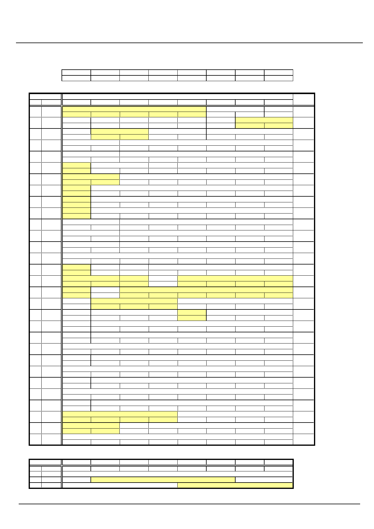
I2C Bus Table
SLAVE ADDRESS= BAH(WRITE), BBH(READ)
A6
A5
A4
A3
A2
A1
A0
R/W
1
0
1
1
1
0
1
1/0
WRITE TABLE(input bytes)
SUB ADDRESS DATA
HEX BIN
D7
D6
D5
00H 00000000
01H 00000001
02H 00000010
04H 00000100
05H 00000101
06H 00000110
07H 00000111
08H 00001000
09H 00001001
0AH 00001010
0BH 00001011
0CH 00001100
0DH 00001101
(not asigned)
0
0
0
X-ray Enable YUV input
Y/C input
0
0
0
Ped Clamp
(not asigned)
0
0
0
Sharpness Delay (Front)
V1
V0
V1
Sharpness Delay (Rear)
V1
V0
V1
(not asigned)
Y DL Time Adj.
V0
V0
V0
(not asigned)
V0
V0
V0
(not asigned)
V0
V0
V1
(not asigned)
V0
V0
V1
(not asigned)
V0
V0
V1
Half Tone
V0
V0
V0
RGB Matrix Ratio
V1
V0
V0
OSD Comp
V0
V0
V0
0EH 00001110
V1
V0
(not asigned)
H Free
0FH 00001111
0
0
(not asigned)
10H 00010000
0
0
(not asigned) Black Stre. SW
11H 00010001
V0
V1
RGB Mute
12H 00010010
1
0
Service SW
13H 00010011
0
0
V-Blanking Stop
14H 00010100
0
1
V-Ramp Invert
15H 00010101
1
1
V0
AFC1 Gain
0
(for evaluation)
0
V0
(inhibited)
0
V-Shift
0
0
1
16H 00010110
V0
V0
V0
CutOff(R) MSB
17H 00010111
V0
V0
V0
18H 00011000
V0
V0
V0
CutOff(G) MSB
19H 00011001
V0
V0
V0
1AH 00011010
1BH 00011011
1CH 00011100
1DH 00011101
V0
V0
V0
CutOff(B) MSB
V0
V0
V0
(not asigned)
0
0
0
(not asigned)
I/M(D) Enable
0
0
0
51H 01010001
0
0
0
READ TABLE(output bytes)
SUB ADDRESS
D7
D6
D5
60H 01100000
61H 01100001
62H 01100010
63H 01100011
KILLER
B2 ROM MSB
H COINCI
V COINCI
BLKDETV
D4
D3
D2
D1
D0
INITIAL
Power Down Mode
H Stop
0
0
0
1
0
EXT input
TV input
Y/C through
(for evaluation)
0
1
0
0
0
VRT Voltage
Sync-tip Clamp
0
1
0
0
0
Shrapness Gain (Front)
V0
V0
V0
V0
V0
Shrapness Gain (Rear)
V0
V0
V0
V0
V0
YNR SW
YNR Limitter Level
V0
V0
V0
V0
V0
Sharpness Limitter Level
V1
V0
V1
V0
V1
Tint Control
V0
V1
V0
V0
V1
Color Control
V0
V1
V0
V0
V0
Contrast Control
V1
V1
V0
V1
V1
OSD Level (R)
V1
V1
V1
V1
V0
OSD Level (G)
V1
V1
V1
V1
V0
OSD Level (B)
V1
V1
V1
V1
V0
Brightness Control
V0
V0
V0
V0
V0
H Phase Control
0
1
0
0
0
2D Y/C
(for evaluation)
0
0
0
0
0
(for evaluation)
V0
V0
V0
V0
V0
Gamma Control
0
0
0
0
0
(inhibited)
Hold Down Level
1
0
0
0
0
V-Ramp Size
0
0
0
0
0
V-Ramp Linearity
1
1
1
1
1
Cut Off (R)
V0
V0
V0
V0
V0
Drive (R)
V0
V0
V0
V0
V0
Cut Off (G)
V0
V0
V0
V0
V0
Drive (G)
V0
V0
V0
V0
V0
Cut Off (B)
V0
V0
V0
V0
V0
Drive (B)
V0
V0
V0
V0
V0
Intelligent Monitor (Analog)
0
0
0
0
0
Intelligent Monitor (Digital)
0
0
0
0
0
H VCO Adjust
0
0
0
0
0
02H
08H
08H
A0H
A0H
00H
15H
29H
28H
3BH
1EH
5EH
0EH
80H
08H
00H
40H
80H
10H
40H
FFH
00H
00H
00H
00H
00H
00H
00H
00H
00H
NOTE: V0 / V1 ==> V- LATCH BIT
D4
D3
B_W
IIC_STILL
B2 ROM
(not asigned)
D2
MV_180
D1
DET NZ
D0
K_MONI
(not asigned)
C Gain
MITSUBISHI
15
Share Link: 