NX25P10 Ver la hoja de datos (PDF) - Winbond
Número de pieza
componentes Descripción
Fabricante
NX25P10 Datasheet PDF : 35 Pages
| |||
W25P10, W25P20 AND W25P40
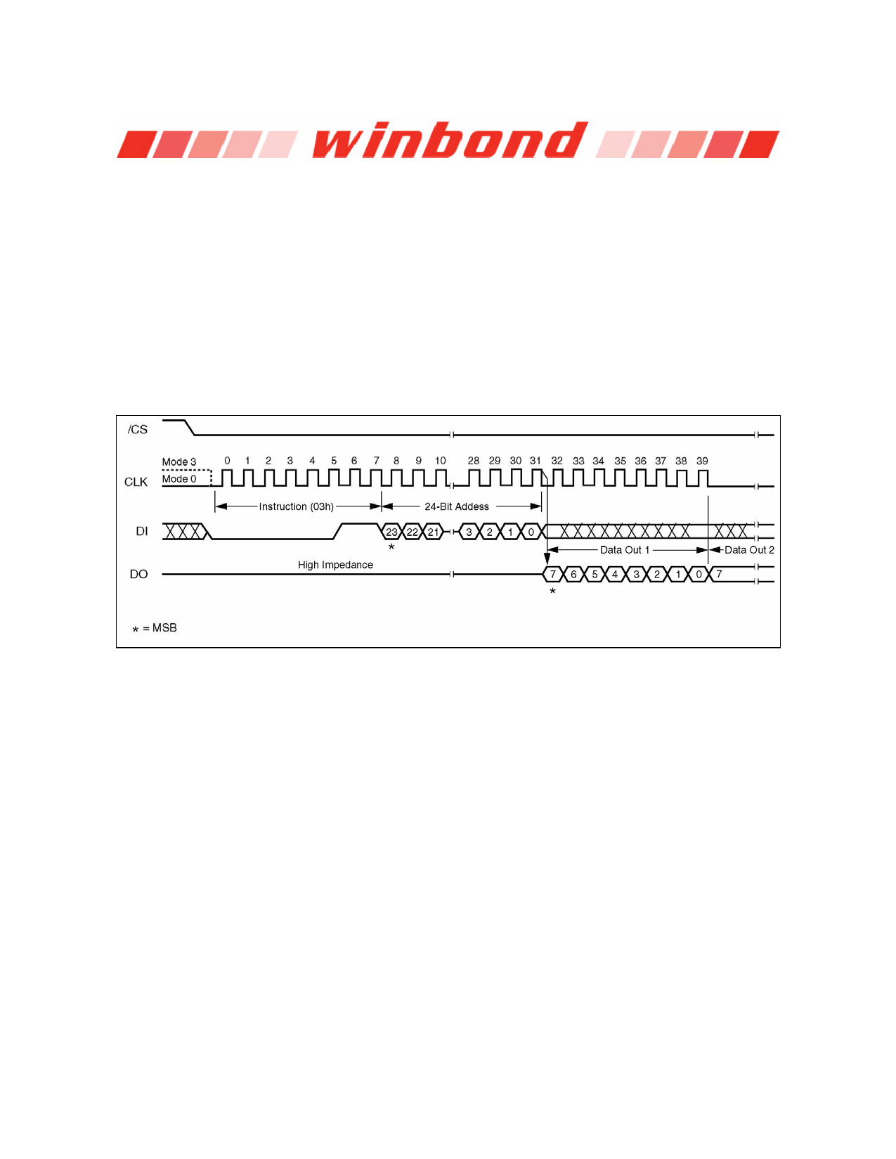
7.2.7 Read Data (03h)
The Read Data instruction allows one or more data bytes to be sequentially read from the memory.
The instruction is initiated by driving the /CS pin low and then shifting the instruction code “03h”
followed by a 24-bit address (A23-A0) into the DI pin. The code and address bits are latched on the
rising edge of the CLK pin. After the address is received, the data byte of the addressed memory
location will be shifted out on the DO pin at the falling edge of CLK with most significant bit (MSB) first.
The address is automatically incremented to the next higher address after each byte of data is shifted
out allowing for a continuous stream of data. This means that the entire memory can be accessed with
a single instruction as long as the clock continues. The instruction is completed by driving /CS high.
The Read Data instruction sequence is shown in figure 8. If a Read Data instruction is issued while an
Erase, Program or Write cycle is in process (BUSY=1) the instruction is ignored and will not have any
effects on the current cycle. The Read Data instruction allows clock rates from D.C. to a maximum of
fR (see AC Electrical Characteristics).
Figure 8. Read Data Instruction Sequence Diagram
- 16 -
Share Link: 