UT2327L-AE3-R(2007) Ver la hoja de datos (PDF) - Unisonic Technologies
Número de pieza
componentes Descripción
Fabricante
UT2327L-AE3-R Datasheet PDF : 5 Pages
| |||
UT2327
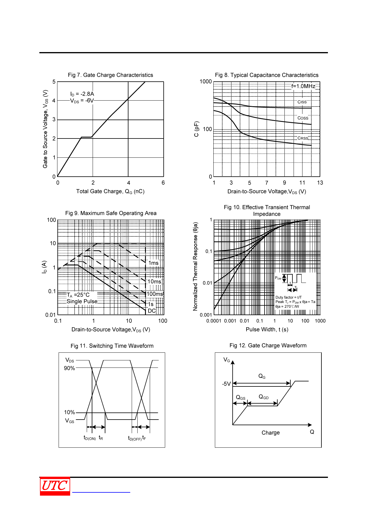
TYPICAL CHARACTERISTICS(Cont.)
Fig 7. Gate Charge Characteristics
5
ID = -2.8A
4
VDS = -6V
3
2
1
0
0
2
4
6
Total Gate Charge, QG (nC)
Fig 9. Maximum Safe Operating Area
100
10
1ms
1
10ms
0.1
TA =25°C
Single Pulse
0.01
0.1
1
100ms
1s
DC
10
100
Drain-to-Source Voltage,VDS (V)
Fig 11. Switching Time Waveform
VDS
90%
10%
VGS
tD(ON) tR
tD(OFF) tF
Power MOSFET
Fig 8. Typical Capacitance Characteristics
1000
f=1.0MHz
CISS
100
COSS
CRSS
0
13
57
9 11 13
Drain-to-Source Voltage,VDS (V)
Fig 10. Effective Transient Thermal
Impedance
1
0.1
0.01
PDM
t
T
Duty factor = t/T
Peak T J = PDM x θja + Ta
θja = 270 ℃/W
0.001
0.0001 0.001 0.01 0.1 1
10 100 1000
Pulse Width, t (s)
Fig 12. Gate Charge Waveform
VG
-5V
QGS
QG
QGD
Charge
Q
UNISONIC TECHNOLOGIES CO., LTD
www.unisonic.com.tw
4 of 5
QW-R502-108,A
Share Link: 