UPD3734ACY Ver la hoja de datos (PDF) - NEC => Renesas Technology
Número de pieza
componentes Descripción
Fabricante
UPD3734ACY Datasheet PDF : 20 Pages
| |||
µPD3734A
6. Output impedance: Zo
Output pin impedance viewed from outside.
7. Response: R
Output voltage divided by exposure (lx·s).
Note that the response varies with a light source.
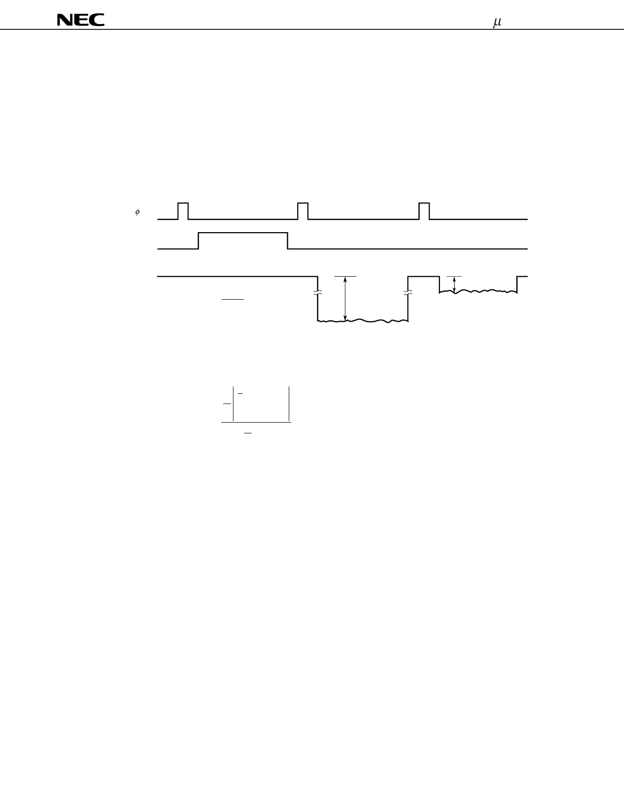
8. Image Lag: IL
The rate between the last output voltage and the next one after read out the data of a line.
φ TG
Light
ON
OFF
VOUT
V1
IL (%) = V1 × 100
VOUT
VOUT
9. Register Imbalance: RI
The rate of the difference between the average of the output voltage of Odd and Even pixels, against the
average output voltage of all the valid pixels.
2
n
RI (%) =
n
2
∑ (V2j−1 − V2j )
j=1
1
n
∑
Vj
n j=1
× 100
n : Number of valid pixels
Vj : Output voltage of each pixel
10. Bit Noise: BN
Output signal distribution of a photocell by scan.
11
Share Link: 